
XCVU3P-L2FFVC1517E
| Part Description |
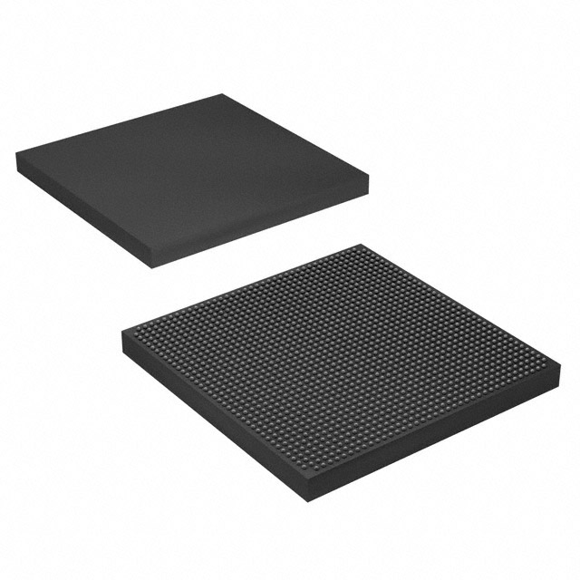
Virtex® UltraScale+™ Field Programmable Gate Array (FPGA) IC 520 130355200 862050 1517-BBGA, FCBGA |
|---|---|
| Quantity | 354 Available (as of June 15, 2026) |

| Product Category | Field Programmable Gate Array (FPGA) |
|---|---|
| Manufacturer | AMD |
| Manufacturing Status | Active |
| Manufacturer Standard Lead Time | 16 Weeks |
| Datasheet |
Specifications & Environmental
| Device Package | 1517-FCBGA (40x40) | Grade | Extended | Operating Temperature | 0°C – 110°C | ||
|---|---|---|---|---|---|---|---|
| Package / Case | 1517-BBGA, FCBGA | Number of I/O | 520 | Voltage | 698 mV - 742 mV | ||
| Mounting Method | Surface Mount | RoHS Compliance | ROHS3 Compliant | REACH Compliance | REACH Unknown | ||
| Moisture Sensitivity Level | 4 (72 Hours) | Number of LABs/CLBs | 49260 | Number of Logic Elements/Cells | 862050 | ||
| Number of Gates | N/A | ECCN | 3A001A7B | HTS Code | 8542.39.0001 | ||
| Qualification | N/A | Total RAM Bits | 130355200 |
Overview of XCVU3P-L2FFVC1517E – Virtex® UltraScale+™ FPGA, 1517-FCBGA (520 I/O)
The XCVU3P-L2FFVC1517E is a Virtex® UltraScale+™ field programmable gate array (FPGA) supplied in a 1517-FCBGA package. It combines a high count of programmable logic resources, substantial embedded memory, and a large I/O complement to address designs that require large-scale, reconfigurable logic and dense system integration.
Key platform attributes include 49,260 CLBs, 862,050 logic elements, approximately 130 Mbits of embedded memory, 520 I/O pins, an extended operating temperature range, and RoHS compliance, enabling deployment in systems that require robust on-chip resources and surface-mount packaging.
Key Features
- Core Logic 49,260 CLBs and 862,050 logic elements provide extensive programmable logic capacity for large designs and complex logic implementations.
- Embedded Memory Approximately 130 Mbits of on-chip RAM (130,355,200 bits) to support buffering, caching, and memory-intensive algorithm implementations.
- I/O 520 general-purpose I/O pins to support wide parallel interfaces, multi-channel connectivity, and high-pin-count boards.
- Power Supply Specified core voltage supply range of 698 mV to 742 mV for the device core power domain.
- Package & Mounting 1517-FCBGA supplier package (40×40) in a 1517-BBGA/FCBGA case, designed for surface-mount placement on PCBs.
- Temperature & Grade Extended grade device with an operating temperature range of 0 °C to 110 °C.
- Compliance RoHS compliant to meet regulatory environmental requirements for lead-free assembly.
Typical Applications
- High-density programmable logic systems Useful where large numbers of logic elements and CLBs are required to implement complex custom logic and data-paths.
- Memory-intensive designs Suited to applications that need substantial on-chip RAM for buffering, packet processing, or algorithm workspace.
- High I/O count systems Ideal for boards and modules that require many parallel interfaces or multi-channel connectivity with up to 520 I/O pins.
Unique Advantages
- Large logic capacity: 862,050 logic elements give designers the headroom to implement complex, high-function-count designs without partitioning across multiple devices.
- Substantial on-chip memory: Approximately 130 Mbits of embedded RAM reduces dependency on external memory for many buffering and storage needs.
- High I/O density: 520 I/O pins support broad peripheral connectivity and high-bandwidth parallel interfaces on a single device.
- Compact FCBGA packaging: 1517-FCBGA (40×40) package enables surface-mount integration for space-constrained board designs.
- Extended operating range: 0 °C to 110 °C grade provides a wider thermal envelope for demanding system environments.
- Regulatory readiness: RoHS compliance supports lead-free assembly processes.
Why Choose XCVU3P-L2FFVC1517E?
The XCVU3P-L2FFVC1517E positions itself as a high-capacity, tightly integrated FPGA option within the Virtex® UltraScale+™ family, offering a combination of large programmable logic resources, substantial embedded memory, and a high I/O count in a compact surface-mount FCBGA package. Its extended temperature range and RoHS compliance make it suitable for demanding board-level designs that require robust on-chip capabilities.
This device is appropriate for engineering teams and procurement needing a single-device solution to consolidate logic, memory, and I/O requirements—reducing external component count and simplifying board-level design while supporting scalable, reconfigurable implementations.
Request a quote or submit an inquiry to receive pricing and availability information for the XCVU3P-L2FFVC1517E.


Date Founded: 1969
Headquarters: Santa Clara, California, USA
Employees: 25,000+
Revenue: $22.68 Billion
Certifications and Memberships: ISO9001:2015, RoHS, REACH


