
XCVU440-2FLGA2892E
| Part Description |
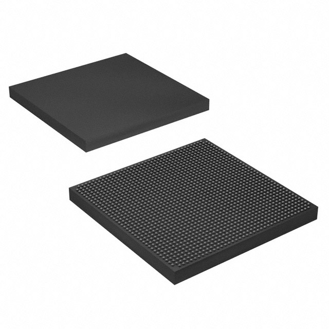
Virtex® UltraScale™ Field Programmable Gate Array (FPGA) IC 1456 90726400 5540850 2892-BBGA, FCBGA |
|---|---|
| Quantity | 1,061 Available (as of June 9, 2026) |

| Product Category | Field Programmable Gate Array (FPGA) |
|---|---|
| Manufacturer | AMD |
| Manufacturing Status | Active |
| Manufacturer Standard Lead Time | 20 Weeks |
| Datasheet |
Specifications & Environmental
| Device Package | 2892-FCBGA (55x55) | Grade | Extended | Operating Temperature | 0°C – 100°C | ||
|---|---|---|---|---|---|---|---|
| Package / Case | 2892-BBGA, FCBGA | Number of I/O | 1456 | Voltage | 922 mV - 979 mV | ||
| Mounting Method | Surface Mount | RoHS Compliance | ROHS3 Compliant | REACH Compliance | REACH Unaffected | ||
| Moisture Sensitivity Level | 4 (72 Hours) | Number of LABs/CLBs | 316620 | Number of Logic Elements/Cells | 5540850 | ||
| Number of Gates | N/A | ECCN | 3A001A7B | HTS Code | 8542.39.0001 | ||
| Qualification | N/A | Total RAM Bits | 90726400 |
Overview of XCVU440-2FLGA2892E – Virtex® UltraScale™ Field Programmable Gate Array (FPGA), 2892-FCBGA
The XCVU440-2FLGA2892E is a Virtex® UltraScale™ Field Programmable Gate Array (FPGA) in a 2892-ball FCBGA package. It delivers a high-density programmable fabric with a large logic element count, substantial on-chip memory, and a high I/O count for system designs that require extensive integration at the chip level.
Key attributes include approximately 5,540,850 logic elements, roughly 90.7 Mbits of embedded memory, and 1,456 I/O pins, making the device suitable for designs that demand large amounts of logic resources, significant embedded RAM, and broad I/O connectivity within a 55×55 mm FCBGA footprint.
Key Features
- Logic Capacity Approximately 5,540,850 logic elements to implement large-scale digital designs and complex programmable logic functions.
- Embedded Memory Approximately 90.7 Mbits of on-chip RAM to support buffering, large lookup tables, and data storage for high-throughput designs.
- High I/O Count 1,456 programmable I/O pins provide extensive external connectivity for multi-channel interfaces and board-level integration.
- Package and Mounting 2892-BBGA / 2892-FCBGA (55×55 mm) surface-mount package for dense board designs where a high-ball-count BGA is required.
- Supply Voltage Range Operates from 922 mV to 979 mV, enabling designers to plan power delivery and regulator selection precisely around the specified core supply window.
- Operating Temperature Rated for operation from 0 °C to 100 °C (Extended grade), allowing deployment in controlled and industrial-adjacent ambient conditions.
- Mounting Type Surface mount package supports standard PCB assembly processes for BGA components.
Typical Applications
- High-density digital systems Implement large-scale custom logic and algorithm acceleration where extensive logic elements and on-chip RAM are required.
- Multi‑channel I/O platforms Use the 1,456 I/O pins to connect numerous interfaces, sensors, or transceivers in data aggregation and signal-routing applications.
- FPGA-based processing modules Deploy as the programmable compute element in modules that need significant embedded memory for buffering and intermediate data storage.
- Board-level integration Leverage the 2892-FCBGA (55×55) package for high-density PCB designs that consolidate multiple functions onto a single FPGA.
Unique Advantages
- Large programmable fabric: A high logic element count enables integration of complex algorithms and multiple subsystems on a single device, reducing component count.
- Substantial on-chip RAM: Approximately 90.7 Mbits of embedded memory simplifies data path design and lowers external memory dependency for many workloads.
- Extensive I/O availability: 1,456 I/Os provide flexibility to interface with numerous peripherals and parallel data channels without external multiplexing.
- Compact high-ball-count package: The 2892-FCBGA (55×55) package provides a dense pinout that supports complex routing and high-pin-count designs in a single footprint.
- Defined supply and thermal envelope: Clear voltage supply range (922 mV–979 mV) and operating temperature (0 °C–100 °C) allow precise system-level power and thermal planning.
Why Choose XCVU440-2FLGA2892E?
The XCVU440-2FLGA2892E positions itself as a high-density Virtex UltraScale FPGA option for projects that require extensive logic resources, significant embedded memory, and broad I/O capability within an FCBGA package. Its combination of approximately 5.54 million logic elements, roughly 90.7 Mbits of on-chip RAM, and 1,456 I/Os supports consolidation of complex functions into a single programmable device.
This device is suitable for engineering teams and procurement organizations targeting designs that benefit from high integration density and predictable power/thermal parameters. The extended-grade temperature rating and clearly specified package and supply characteristics help with system validation and deployment planning.
Request a quote or submit a purchase inquiry to obtain pricing, availability, and lead-time details for the XCVU440-2FLGA2892E. Our team can assist with order placement and provide component-level information to support your design and procurement process.


Date Founded: 1969
Headquarters: Santa Clara, California, USA
Employees: 25,000+
Revenue: $22.68 Billion
Certifications and Memberships: ISO9001:2015, RoHS, REACH


