
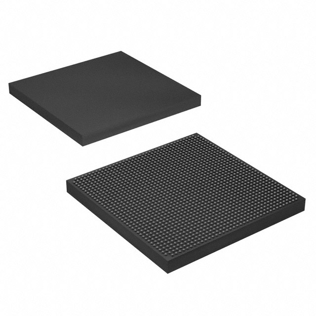
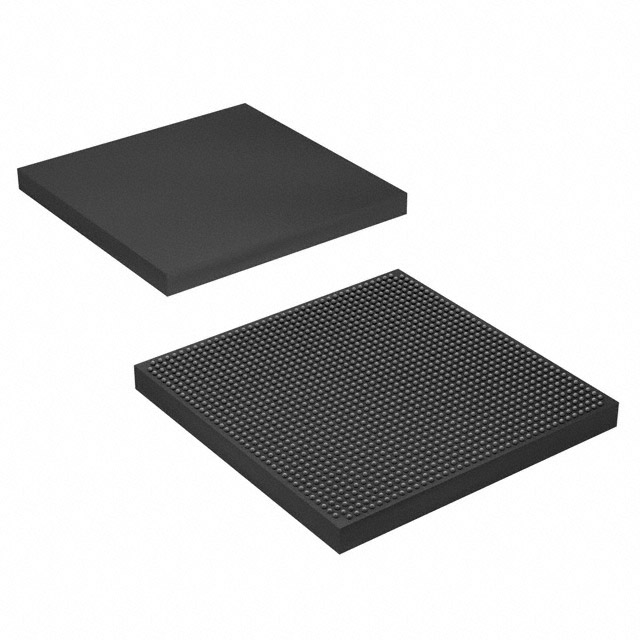
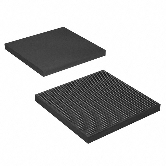
XCVU440-1FLGA2892C
| Part Description |
Virtex® UltraScale™ Field Programmable Gate Array (FPGA) IC 1456 90726400 5540850 2892-BBGA, FCBGA |
|---|---|
| Quantity | 368 Available (as of October 8, 2026) |

| Product Category | Field Programmable Gate Array (FPGA) |
|---|---|
| Manufacturer | AMD |
| Manufacturing Status | Active |
| Manufacturer Standard Lead Time | 20 Weeks |
| Datasheet |
Specifications & Environmental
| Device Package | 2892-FCBGA (55x55) | Grade | Commercial | Operating Temperature | 0°C – 85°C | ||
|---|---|---|---|---|---|---|---|
| Package / Case | 2892-BBGA, FCBGA | Number of I/O | 1456 | Voltage | 922 mV - 979 mV | ||
| Mounting Method | Surface Mount | RoHS Compliance | ROHS3 Compliant | REACH Compliance | REACH Unaffected | ||
| Moisture Sensitivity Level | 4 (72 Hours) | Number of LABs/CLBs | 316620 | Number of Logic Elements/Cells | 5540850 | ||
| Number of Gates | N/A | ECCN | 3A001A7B | HTS Code | 8542.39.0001 | ||
| Qualification | N/A | Total RAM Bits | 90726400 |
Overview of XCVU440-1FLGA2892C – Virtex® UltraScale™ FPGA, 2892‑FCBGA, Commercial Grade
The XCVU440-1FLGA2892C is a Virtex® UltraScale™ Field Programmable Gate Array (FPGA) in a 2892‑FCBGA (55×55) surface-mount package. It provides a very high logic capacity combined with substantial on-chip memory and a large number of I/O, targeting designs that require dense programmable logic and significant embedded memory.
With 316,620 CLBs, approximately 5,540,850 logic elements and roughly 90.7 Mbits of embedded memory, this commercial‑grade FPGA is suited for applications that need high integration, flexible I/O routing and low-voltage operation within a 0 °C to 85 °C operating range.
Key Features
- Core Logic: 316,620 CLBs and 5,540,850 logic elements provide extensive programmable fabric for large, complex designs and parallel implementations.
- Embedded Memory: Approximately 90.7 Mbits of on‑chip RAM to support buffering, large lookup tables and memory‑heavy algorithms without external SDRAM for some workloads.
- I/O Density: 1,456 I/O pins to support broad interfacing requirements and high‑channel count designs.
- Package & Mounting: 2892‑FCBGA (55×55) package in a surface‑mount form factor for compact, high‑density board layouts.
- Power Supply Range: Low‑voltage core operation from 922 mV to 979 mV enabling designs optimized for reduced core voltage domains.
- Temperature & Grade: Commercial grade operation from 0 °C to 85 °C; RoHS compliant.
Typical Applications
- High‑density digital processing: Use the large logic and memory resources to implement complex signal processing and algorithm acceleration that require substantial on‑chip resources.
- Prototyping and system emulation: High logic capacity and abundant I/O make this FPGA suitable for developing and validating large systems before ASIC implementation.
- Data buffering and packet handling: Significant embedded RAM and many I/O support high‑throughput buffering, packet aggregation and interface bridging functions.
Unique Advantages
- High logic integration: Hundreds of thousands of CLBs and millions of logic elements reduce the need for multiple devices and simplify partitioning of large designs.
- Substantial on‑chip memory: Approximately 90.7 Mbits of embedded RAM enables internal data storage and reduces dependency on external memory for many use cases.
- Extensive I/O count: 1,456 I/O pins allow direct connection to a wide range of peripherals and high‑channel systems without additional interface chips.
- Compact, manufacturable package: 2892‑FCBGA (55×55) surface‑mount package supports dense PCB layouts and standard assembly processes.
- Low core‑voltage operation: Core supply range of 922 mV to 979 mV supports designs targeting low‑voltage power domains.
- RoHS compliant, commercial grade: Meets RoHS requirements and is specified for 0 °C to 85 °C commercial operation.
Why Choose XCVU440-1FLGA2892C?
The XCVU440-1FLGA2892C positions itself as a high‑capacity, commercial‑grade Virtex® UltraScale™ FPGA designed for engineers who require large programmable logic resources, ample embedded memory and a substantial I/O complement in a single device. Its combination of CLBs, logic elements and on‑chip RAM supports consolidation of complex functions onto a single FPGA, reducing board-level complexity.
This part is well suited for teams developing large digital systems, prototype platforms or memory‑intensive logic where scalability and integration can shorten development cycles. The device’s package, voltage range and RoHS compliance help integrate it into standard manufacturing flows while meeting commercial operational requirements.
Request a quote or submit a price inquiry to receive availability and purchasing information for the XCVU440-1FLGA2892C.





















Date Founded: 1969
Headquarters: Santa Clara, California, USA
Employees: 25,000+
Revenue: $22.68 Billion
Certifications and Memberships: ISO9001:2015, RoHS, REACH











