
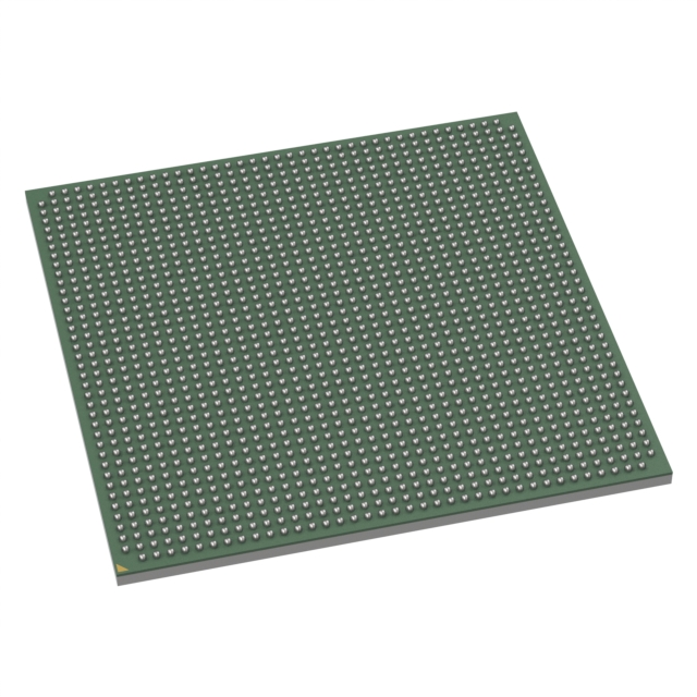
LX2160SC72232B
| Part Description |
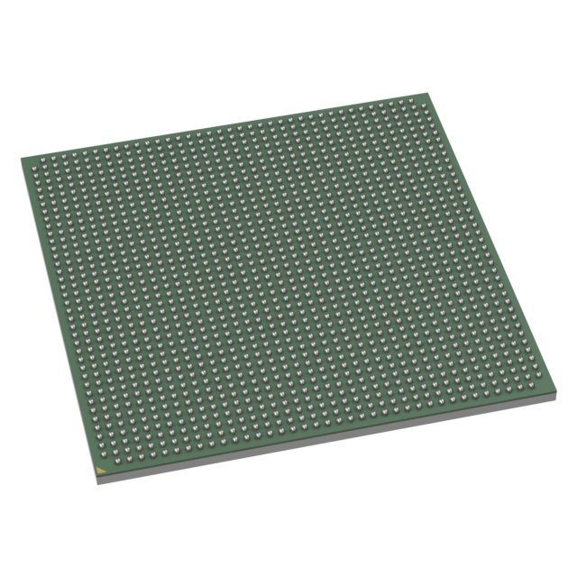
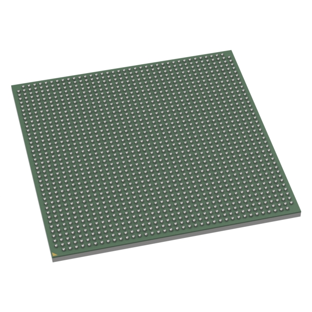
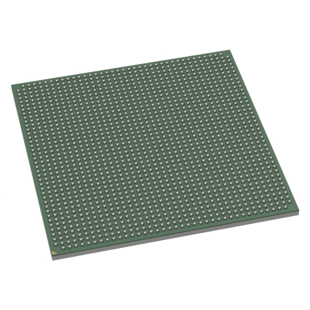
ARM® Cortex®-A72 Microprocessor IC QorlQ LX2 16 Core, 64-Bit 2.2GHz 1517-FCPBGA (40x40) |
|---|---|
| Quantity | 1,349 Available (as of October 8, 2026) |
| Product Category | Microprocessors |
|---|---|
| Part Series | LX2160S |
| Manufacturer | NXP USA Inc. |
| Manufacturing Status | Active |
| Manufacturer Standard Lead Time | 18 Weeks |
| Datasheet |
Specifications & Environmental
| Core Processor | ARM® Cortex®-A72 | Device Package | 1517-FCPBGA (40x40) | ECCN | 5A002A1 NXP | ||
|---|---|---|---|---|---|---|---|
| Ethernet | 100Gbps (2) | Graphics Acceleration | Yes | HTS Code | 8542.31.0001 | ||
| Moisture Sensitivity Level | N/A | Mounting Method | Surface Mount | Mounting Type | Surface Mount | ||
| Number of Cores/Bus Width | 16 Core, 64-Bit | Operating Temperature | 0°C ~ 105°C (TJ) | Package / Case | 1517-BBGA, FCBGA | ||
| RAM Controllers | DDR4 | REACH Compliance | REACH Unaffected | RoHS Compliance | ROHS3 Compliant | ||
| SATA | SATA 3.0 (4) | Security Features | Secure Boot, TrustZone® | Speed | 2.2GHz | ||
| Supplier Device Package | 1517-FCPBGA (40×40) | USB | USB 3.0 (2) + PHY (2) | Voltage – I/O | 1.2V, 1.8V, 3.3V |
Overview of LX2160SC72232B – IC MPU QORLQ 2.2GHZ 1517FCPBGA
The LX2160SC72232B is an NXP Layerscape LX2160A-series microprocessor IC featuring sixteen 64-bit ARM® Cortex®-A72 cores running up to 2.2 GHz in a 1517-FCPBGA (40 × 40) package. It is engineered for compute-intensive networking and edge processing applications that require high integration, multi‑core performance, and extensive I/O.
Designed to consolidate control-plane and data-plane functions, this device targets use cases such as networking, data center offload and 5G packet processing, delivering integrated packet caching, high-speed SerDes and multi‑100 Gbit/s class connectivity while supporting secure boot and TrustZone® security features.
Key Features
- CPU Cores Sixteen 64-bit ARMv8 Cortex-A72 cores running up to 2.2 GHz for multi-threaded compute performance.
- On-chip Cache 16 MB of cache to support low-latency processing and high throughput workloads.
- Memory Subsystem Dual DDR4 72-bit controllers with ECC support, capable of up to 3200 MT/s and a maximum memory capacity cited as 256 GB.
- Packet Caching 2 MB on-chip packet caching buffer to minimize external memory usage and reduce latency for packet handling.
- High-speed SerDes 24 SerDes lanes operating up to 25 GHz to enable high-bandwidth external interfaces and board-level scalability.
- Ethernet and Switching Integrated networking with support for up to 16 Ethernet ports, including dual 100 Gbit/s Ethernet and a 122 Gbit/s Layer‑2 switch.
- Security and Offload 50 Gbit/s security accelerator plus support for Secure Boot and Arm TrustZone® for hardware-enabled platform security.
- Data Compression 100 Gbit/s compression/decompression engine to offload data-reduction tasks from general-purpose cores.
- Peripheral and I/O Up to 24 PCIe Gen3 lanes, 4 × SATA 3.0, 2 × USB 3.0 + PHY, SD/eMMC, DUART, I²C, and CAN interfaces (CAN FD optional noted in documentation).
- Package & Environmental 1517-FCPBGA (40 × 40) surface-mount package; operating temperature range 0 °C to 105 °C. RoHS compliant.
- Qualification Device qualification listed as Consumer in the product data.
Typical Applications
- Networking Control and Data Plane — Multi-core processing and integrated Layer‑2 switching enable control-plane and data-plane consolidation on a single SoC.
- Data Center Offload — High-speed I/O, PCIe lanes and compression/security accelerators support offload tasks and NIC-style architectures.
- 5G Packet Processing — Architecture and accelerators are suited to packet processing and protocol offload in 5G edge and central units.
- Industrial Edge Processing — High integration and robust operating range support compute-intensive edge functions and protocol bridging.
Unique Advantages
- Highly integrated compute and I/O: Sixteen Cortex‑A72 cores combined with multi‑100 Gbit/s Ethernet, SerDes and PCIe reduce component count and board complexity.
- On-chip packet buffering: The 2 MB packet cache lowers external memory bandwidth needs, reducing latency and power for packet processing workloads.
- Hardware accelerators: Built-in 50 Gbit/s security and 100 Gbit/s compression engines offload intensive tasks from cores to improve overall throughput.
- Broad protocol support: Multiple high-speed interfaces (Ethernet, PCIe, SATA, USB, CAN) provide flexibility for diverse system architectures.
- Developer ecosystem: Documentation references support from a Linux SDK and embedded development tools for Layerscape processors to accelerate software bring-up.
- Long-term availability: Product documentation cites product longevity planning to help support long-life deployments.
Why Choose LX2160SC72232B?
The LX2160SC72232B positions high multi-core compute density alongside extensive, high-bandwidth I/O and dedicated accelerators—making it suitable for designs that require consolidated networking, security and data offload capability in a single package. Its on-chip packet caching, integrated switch capabilities and robust memory subsystem help reduce external memory and interface complexity while supporting demanding throughput requirements.
This device is appropriate for teams building networking, edge compute and 5G packet-processing systems that need a combination of CPU performance, integrated accelerators and broad interface support, backed by Layerscape software resources to accelerate development and deployment.
Request a quote or submit an inquiry to obtain pricing, availability and lead-time information for the LX2160SC72232B. Our team can provide the details you need to evaluate this processor in your design.



















Date Founded: 2006
Headquarters: Eindhoven, North Brabant, Netherlands
Employees: 38,000+
Revenue: $10.53 Billion
Certifications and Memberships: ISO9001:2015, IATF16949:2016


