
MPC8265AVVPIBC
| Part Description |
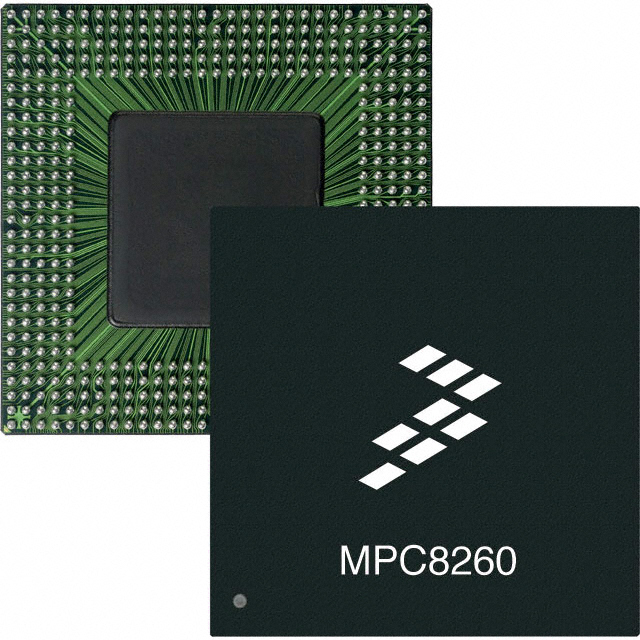
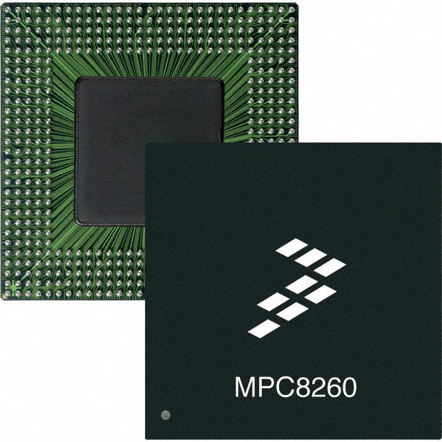
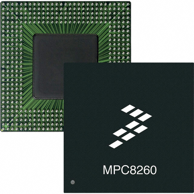
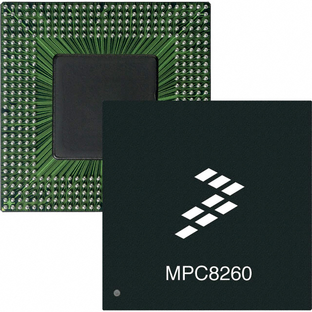
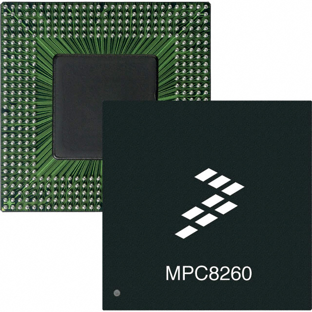
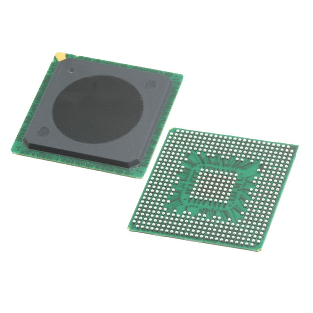
PowerPC G2 Microprocessor IC MPC82xx 1 Core, 32-Bit 300MHz 480-TBGA (37.5x37.5) |
|---|---|
| Quantity | 267 Available (as of October 8, 2026) |
| Product Category | Microprocessors |
|---|---|
| Part Series | MPC8265 |
| Manufacturer | NXP USA Inc. |
| Manufacturing Status | Obsolete |
| Manufacturer Standard Lead Time | Contact Us |
| Datasheet |
Specifications & Environmental
| Co-Processors/DSP | Communications; RISC CPM | Core Processor | PowerPC G2 | Device Package | 480-TBGA (37.5x37.5) | ||
|---|---|---|---|---|---|---|---|
| ECCN | 5A991B4B | Ethernet | 10/100Mbps (3) | Graphics Acceleration | No | ||
| HTS Code | 8542.31.0001 | Moisture Sensitivity Level | 3 (168 Hours) | Mounting Method | Surface Mount | ||
| Mounting Type | Surface Mount | Number of Cores/Bus Width | 1 Core, 32-Bit | Operating Temperature | 0°C ~ 105°C (TA) | ||
| Package / Case | 480-LBGA Exposed Pad | RAM Controllers | DRAM, SDRAM | REACH Compliance | REACH Unaffected | ||
| RoHS Compliance | ROHS3 Compliant | Speed | 300MHz | Supplier Device Package | 480-TBGA (37.5×37.5) | ||
| Voltage – I/O | 3.3V |
Overview of MPC8265AVVPIBC – IC MPU MPC82XX 300MHZ 480TBGA
The MPC8265AVVPIBC is a PowerPC G2-based 32-bit microprocessor operating at 300 MHz, designed for embedded communications and protocol processing. As a member of the MPC82xx/PowerQUICC II family from NXP Semiconductors, it combines a high-performance PowerPC G2 core with integrated communications peripherals and memory controller support to address embedded networking and protocol offload tasks.
Built for surface-mount PCB integration in a 480-TBGA (37.5 × 37.5 mm) package and qualified for consumer applications, the device offers a compact platform for designs that require integrated Ethernet, CPM-based communications acceleration, and flexible memory interfacing.
Key Features
- Core & Performance Dual-issue PowerPC G2 architecture, 1 core, 32-bit operation at 300 MHz delivering predictable embedded processing performance.
- On-chip CPU Resources Family-level features include separate 16 KB instruction and 16 KB data caches and a floating-point unit (as described in the MPC826xA family documentation).
- Communications Co-Processors Integrated communications co-processors and a RISC Communication Processor Module (CPM) for protocol handling and offload functions.
- Ethernet 10/100 Mbps Ethernet capability as listed in the product specifications (10/100Mbps (3)).
- Memory Support On-chip controllers for DRAM and SDRAM to support system memory requirements.
- Serial & Auxiliary Interfaces Additional interfaces include I2C and serial peripheral support suitable for system control and peripheral integration.
- Powering & Clocking 3.3 V I/O voltage and family-level design features such as separate power supplies for internal logic and I/O plus configurable clock multipliers to enable power/performance tuning.
- Package & Mounting 480-lead TBGA exposed-pad package (37.5 × 37.5 mm), surface-mount mounting for compact, production-ready board designs.
- Operating Range & Compliance Operating temperature range 0 °C to 105 °C and RoHS compliant.
Typical Applications
- Embedded Networking Equipment Protocol processing, packet handling and control in routers, managed switches and Ethernet-enabled appliances leveraging integrated CPM and 10/100 Mbps Ethernet.
- Communications Controllers Offloading serial and protocol tasks via the CPM and communications co-processor building blocks for telecom or data communication endpoints.
- Embedded Systems with SDRAM/DRAM Systems requiring on-chip memory controller support for DRAM/SDRAM and deterministic CPU and cache behavior for real-time embedded tasks.
Unique Advantages
- Integrated Communications Subsystem On-chip CPM and communications co-processors reduce external logic and simplify protocol offload designs.
- Balanced Performance and Efficiency PowerPC G2 core at 300 MHz with separate caches and an FPU (family-level feature) provides a balance of integer and floating-point capability for embedded workloads.
- Flexible Memory and I/O Built-in DRAM/SDRAM controllers and serial interfaces like I2C streamline system memory and peripheral integration.
- Design-Ready Packaging 480-TBGA exposed-pad, surface-mount package supports compact PCB layouts and thermal conduction for production systems.
- Power and Clock Configuration Separate supplies for core and I/O plus configurable clock multipliers (family-level capabilities) enable designers to tune power versus performance.
- Regulatory and Environmental Compatibility RoHS compliance supports environmentally conscious manufacturing and supply chain requirements.
Why Choose MPC8265AVVPIBC?
The MPC8265AVVPIBC positions itself as a capable embedded communications processor that combines a 300 MHz PowerPC G2 core with integrated communications accelerators and memory controller support. Its family-level PowerQUICC II heritage provides documented architectural features such as CPM-based protocol handling, separate instruction/data caches, and clocking flexibility that help simplify system architecture for networking and protocol-driven designs.
This part is well suited for designers and procurement teams targeting consumer-qualified embedded networking and communications products that require integrated Ethernet capability, reliable memory interfacing, and a compact TBGA footprint backed by NXP Semiconductors' MPC82xx family documentation.
Request a quote or submit an RFQ for the MPC8265AVVPIBC to check pricing and availability for your next embedded communications design.





















Date Founded: 2006
Headquarters: Eindhoven, North Brabant, Netherlands
Employees: 38,000+
Revenue: $10.53 Billion
Certifications and Memberships: ISO9001:2015, IATF16949:2016


