
10M08SAU169I7P
| Part Description |
MAX® 10 Field Programmable Gate Array (FPGA) IC 130 387072 8000 169-LFBGA |
|---|---|
| Quantity | 503 Available (as of June 9, 2026) |

| Product Category | Field Programmable Gate Array (FPGA) |
|---|---|
| Manufacturer | Intel |
| Manufacturing Status | Active |
| Manufacturer Standard Lead Time | 12 Weeks |
| Datasheet |
Specifications & Environmental
| Device Package | 169-UBGA (11x11) | Grade | Industrial | Operating Temperature | -40°C – 100°C | ||
|---|---|---|---|---|---|---|---|
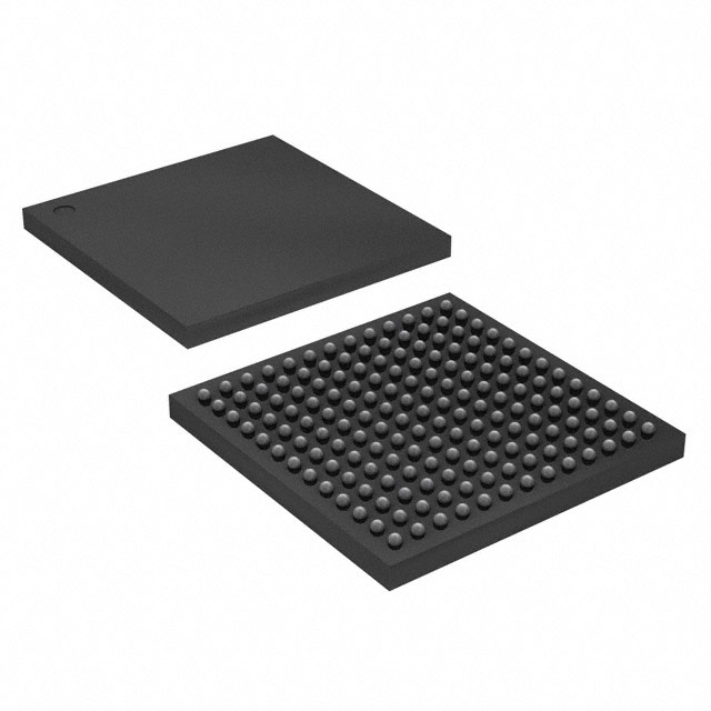
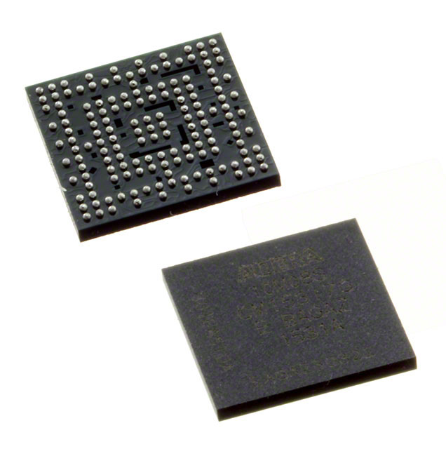
| Package / Case | 169-LFBGA | Number of I/O | 130 | Voltage | 2.85 V - 3.465 V | ||
| Mounting Method | Surface Mount | RoHS Compliance | RoHS non-compliant | REACH Compliance | REACH Unaffected | ||
| Moisture Sensitivity Level | 3 (168 Hours) | Number of LABs/CLBs | 500 | Number of Logic Elements/Cells | 8000 | ||
| Number of Gates | N/A | ECCN | 5A002A1 | HTS Code | 8542.39.0001 | ||
| Qualification | N/A | Total RAM Bits | 387072 |
Overview of 10M08SAU169I7P – MAX® 10 Field Programmable Gate Array (FPGA) IC 130 387072 8000 169-LFBGA
The 10M08SAU169I7P is an Intel MAX® 10 FPGA device delivering a mid-range, non-volatile FPGA fabric with on-chip memory and flexible I/O for industrial applications. It integrates 8,000 logic elements, 387,072 total RAM bits, and up to 130 I/O pins in a compact 169-ball LFBGA package.
Designed for use where configurable logic, embedded memory, and a broad operating temperature range are required, this device supports deployment across industrial systems that demand ruggedized temperature performance and a surface-mount package for compact PCB designs.
Key Features
- Logic Capacity 8,000 logic elements provide mid-range programmable logic density for combinational and sequential designs.
- Logic Array Blocks (LABs) 500 LABs (logic array blocks) for organized logic partitioning and resource allocation.
- On-Chip Memory 387,072 total RAM bits enable local buffering, FIFOs, and small embedded data stores without external memory.
- I/O Count 130 I/O pins support multiple external peripherals and parallel interfaces directly from the FPGA fabric.
- Power and Supply Supports a supply voltage range of 2.85 V to 3.465 V for core and I/O domain flexibility within specified system rails.
- Package & Mounting 169-LFBGA (169-UBGA, 11×11) surface-mount package suitable for space-constrained PCB layouts.
- Temperature & Grade Industrial grade with an operating temperature range of −40 °C to 100 °C for deployment in thermally demanding environments.
- Compliance RoHS compliant for environmental and regulatory alignment.
Typical Applications
- Industrial Control Programmable logic and 130 I/Os allow implementation of control logic, motor interfaces, and deterministic I/O handling in industrial systems operating across −40 °C to 100 °C.
- Embedded Processing Use the 8,000 logic elements and on-chip RAM for embedded state machines, pre-processing, and protocol bridging within compact systems.
- Sensor and Data Aggregation On-chip RAM and numerous I/Os support aggregation, buffering, and preprocessing of sensor data before handing off to host processors.
- Human–Machine Interfaces (HMI) Drive and manage displays, keypads, and peripheral interfaces with dedicated I/O and programmable logic for custom UI control.
Unique Advantages
- Balanced Logic and Memory: 8,000 logic elements paired with 387,072 RAM bits let you partition functions between logic and on-chip storage without relying on external memory for many applications.
- Generous I/O Density: 130 I/Os provide flexible connectivity to sensors, actuators, displays, and communication peripherals, reducing the need for additional interface chips.
- Industrial-Grade Temperature Range: Rated from −40 °C to 100 °C to meet the thermal requirements of industrial deployments.
- Compact Surface-Mount Packaging: 169-LFBGA (11×11 UBGA) delivers a small PCB footprint for space-constrained designs while maintaining routing density.
- Wide Supply Voltage Support: Operates across a 2.85 V to 3.465 V supply range to accommodate common system rails.
- RoHS Compliant: Meets RoHS requirements for environmentally conscious designs and regulatory compliance.
Why Choose 10M08SAU169I7P?
The 10M08SAU169I7P positions itself as a compact, industrial-grade FPGA option that combines moderate logic density, substantive on-chip RAM, and a high I/O count in a surface-mount LFBGA package. Its specified operating range and RoHS compliance make it suitable for designs that require reliable programmable logic in temperature-demanding environments.
This device is well suited to engineers and procurement teams seeking a configurable hardware building block for industrial control, embedded processing, and peripheral aggregation where on-chip memory and flexible I/O reduce external component count and simplify board-level design.
Request a quote or submit an inquiry to get pricing and availability for the 10M08SAU169I7P and begin integrating this Intel MAX® 10 FPGA into your next industrial design.


Date Founded: 1968
Headquarters: Santa Clara, California, USA
Employees: 130,000+
Revenue: $54.23 Billion
Certifications and Memberships: ISO9001:2015, ISO14001:2015, ISO17025:2017, ISO27001:2022, ISO45001:2018, ISO50001:2018


