
5SGSMD3H2F35C1WN
| Part Description |
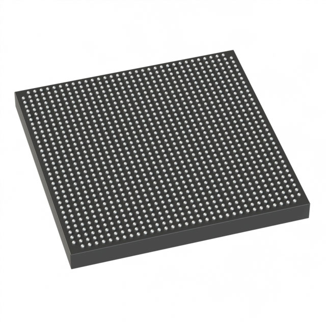
Stratix® V GS Field Programmable Gate Array (FPGA) IC 432 13312000 236000 1152-BBGA, FCBGA |
|---|---|
| Quantity | 195 Available (as of June 10, 2026) |

| Product Category | Field Programmable Gate Array (FPGA) |
|---|---|
| Manufacturer | Intel |
| Manufacturing Status | Obsolete |
| Manufacturer Standard Lead Time | Contact Us |
| Datasheet |
Specifications & Environmental
| Device Package | 1152-FBGA (35x35) | Grade | Commercial | Operating Temperature | 0°C – 85°C | ||
|---|---|---|---|---|---|---|---|
| Package / Case | 1152-BBGA, FCBGA | Number of I/O | 432 | Voltage | 870 mV - 930 mV | ||
| Mounting Method | Surface Mount | RoHS Compliance | RoHS non-compliant | REACH Compliance | REACH Unknown | ||
| Moisture Sensitivity Level | 4 (72 Hours) | Number of LABs/CLBs | 89000 | Number of Logic Elements/Cells | 236000 | ||
| Number of Gates | N/A | ECCN | OBSOLETE | HTS Code | N/A | ||
| Qualification | N/A | Total RAM Bits | 13312000 |
Overview of 5SGSMD3H2F35C1WN – Stratix® V GS Field Programmable Gate Array (FPGA)
The 5SGSMD3H2F35C1WN is a Stratix V GS family FPGA from Intel, supplied in a 1152-BBGA (35×35) FCBGA package for surface-mount assembly. It delivers a combination of large programmable logic capacity, substantial on‑chip memory, and high I/O count targeted at complex commercial digital designs.
Its feature set — including approximately 236,000 logic elements, roughly 13.3 Mbits of embedded memory, and 432 user I/Os — makes it suitable for designs that require high integration density within a single-package programmable device while operating within commercial temperature and voltage ranges.
Key Features
- Core logic Approximately 236,000 logic elements (cells) to implement large-scale custom logic and control functions.
- Embedded memory Approximately 13.3 Mbits of on-chip RAM for buffering, packet storage, and intermediate data processing.
- I/O density 432 user I/Os to support wide buses, parallel interfaces, and multiple peripheral connections.
- Package & mounting 1152-BBGA (FBGA, 35×35) FCBGA package designed for surface-mount board assembly.
- Power Core supply voltage range 870 mV to 930 mV, enabling defined power delivery and regulation design.
- Commercial temperature grade Rated for operation from 0 °C to 85 °C, suitable for commercial-environment systems.
- Compliance RoHS compliant for environmental and regulatory alignment.
Typical Applications
- High-density digital logic Implement large, custom digital functions using the device’s approximately 236,000 logic elements.
- Memory-intensive buffering Use the approximately 13.3 Mbits of embedded RAM for packet buffering, FIFOs, and on-chip data staging.
- I/O-rich system interfaces Integrate wide parallel buses or many peripheral connections using the 432 available I/Os.
- Compact system integration Deploy in space-constrained designs with the 1152-BBGA (35×35) surface-mount package to minimize board area.
Unique Advantages
- Substantial programmable capacity: Approximately 236,000 logic elements enable complex custom logic consolidation into a single FPGA, reducing external component count.
- Significant on-chip memory: Approximately 13.3 Mbits of embedded RAM supports local buffering and memory-intensive algorithms without immediate external memory dependence.
- High I/O count: 432 I/Os provide flexibility for parallel interfaces and mixed-signal front-end connections, simplifying board-level routing.
- Space-efficient packaging: The 1152-BBGA (35×35) FCBGA package supports dense board integration while remaining compatible with standard surface-mount assembly.
- Commercial-environment ready: Rated for 0 °C to 85 °C operation and RoHS compliant to meet common commercial product and regulatory needs.
- Defined core power window: Core supply specification of 870 mV–930 mV helps guide power-supply design and thermal budgeting for predictable operation.
Why Choose 5SGSMD3H2F35C1WN?
The 5SGSMD3H2F35C1WN places substantial logic density, on-chip memory, and a high I/O count into a single commercial-grade, surface-mount FCBGA package. This combination supports consolidation of complex digital subsystems and memory buffers into one programmable device, simplifying BOMs and enabling tighter integration.
It is well suited for engineers and teams designing commercial electronic systems that require large programmable logic capacity, significant embedded RAM, and flexible interfacing within a 0 °C to 85 °C operating window. The device’s package and power specifications provide clear parameters for board layout and power delivery planning.
Request a quote or submit an inquiry to receive pricing, availability, and technical ordering details for the 5SGSMD3H2F35C1WN.


Date Founded: 1968
Headquarters: Santa Clara, California, USA
Employees: 130,000+
Revenue: $54.23 Billion
Certifications and Memberships: ISO9001:2015, ISO14001:2015, ISO17025:2017, ISO27001:2022, ISO45001:2018, ISO50001:2018


