
5SGXEA7H3F35C4
| Part Description |
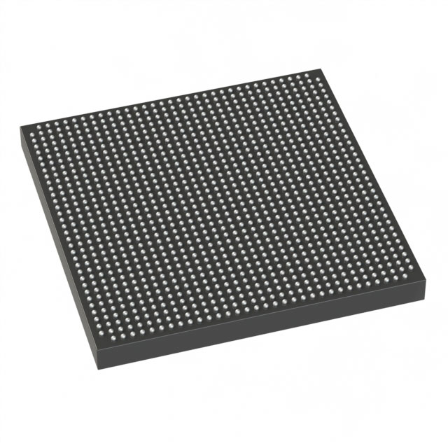
Stratix® V GX Field Programmable Gate Array (FPGA) IC 552 51200000 622000 1152-BBGA, FCBGA |
|---|---|
| Quantity | 789 Available (as of June 10, 2026) |

| Product Category | Field Programmable Gate Array (FPGA) |
|---|---|
| Manufacturer | Intel |
| Manufacturing Status | Obsolete |
| Manufacturer Standard Lead Time | Contact Us |
| Datasheet |
Specifications & Environmental
| Device Package | 1152-FBGA (35x35) | Grade | Commercial | Operating Temperature | 0°C – 85°C | ||
|---|---|---|---|---|---|---|---|
| Package / Case | 1152-BBGA, FCBGA | Number of I/O | 552 | Voltage | 820 mV - 880 mV | ||
| Mounting Method | Surface Mount | RoHS Compliance | RoHS Compliant | REACH Compliance | REACH Unknown | ||
| Moisture Sensitivity Level | 3 (168 Hours) | Number of LABs/CLBs | 234720 | Number of Logic Elements/Cells | 622000 | ||
| Number of Gates | N/A | ECCN | 3A001A2C | HTS Code | 8542.39.0001 | ||
| Qualification | N/A | Total RAM Bits | 51200000 |
Overview of 5SGXEA7H3F35C4 – Stratix® V GX Field Programmable Gate Array (FPGA) IC 552 51200000 622000 1152-BBGA, FCBGA
The 5SGXEA7H3F35C4 is an Intel Stratix V GX family FPGA delivering high-density programmable logic and embedded memory in a 1152-ball FCBGA package. It combines large logic capacity and substantial on-chip RAM with a rich I/O count and commercial-temperature grading for demanding board-level digital designs.
Device electrical and switching characteristics—including core operating conditions and transceiver-related specifications—are documented in the Stratix V device datasheet, enabling design validation around performance, power, and I/O timing.
Key Features
- Logic Capacity Approximately 622,000 logic elements for implementing large-scale digital designs and complex algorithms.
- Embedded Memory Approximately 51.2 Mbits of on-chip RAM to support buffering, large state machines, and memory-intensive processing.
- I/O Resources 552 user I/O pins to support broad peripheral and system interfacing requirements.
- Package and Mounting 1152-ball BGA (FCBGA) in a 35 × 35 mm supplier package; surface-mount mounting for standard PCB assembly flows.
- Core Voltage Core supply range specified at 820 mV to 880 mV to define power-supply requirements for the FPGA core.
- Temperature and Grade Commercial-grade device with an operating temperature range of 0 °C to 85 °C.
- Transceiver and Switching Characteristics Stratix V GX family documentation covers transceiver specifications and switching characteristics for timing and signal integrity planning.
- Environmental Compliance RoHS compliant.
Typical Applications
- High-density digital systems Implement large-scale logic and complex control functions using the device’s ~622k logic elements and extensive embedded memory.
- High-bandwidth I/O aggregation Leverage 552 I/O pins to interface multiple peripherals, external memories, and high-pin-count subsystems.
- Board-level FPGA solutions Surface-mount 1152-ball FCBGA packaging supports compact PCB designs that require significant programmable logic and memory on‑chip.
Unique Advantages
- Substantial logic resources: The large logic element count enables complex IP integration and extensive custom logic implementations without immediate part scaling.
- Significant on-chip memory: Approximately 51.2 Mbits of embedded RAM reduces dependence on off-chip memory for many buffering and state-storage tasks.
- High I/O density: 552 I/O pins provide flexibility to connect to a variety of peripherals and high-pin-count interfaces directly.
- Robust package option for dense designs: 1152-ball FCBGA (35 × 35) provides a compact, board-friendly footprint for high-density systems.
- Documented electrical and switching data: Datasheet coverage of operating conditions, power, and transceiver characteristics supports accurate system-level design and validation.
- RoHS compliant: Meets environmental compliance expectations for many commercial product lines.
Why Choose 5SGXEA7H3F35C4?
The 5SGXEA7H3F35C4 positions itself as a high-density, commercially graded Stratix V GX FPGA that balances large programmable logic and embedded memory with a substantial I/O complement and industry-standard FCBGA packaging. Its documented electrical and switching characteristics help engineers define power, timing, and signal-integrity margins during system design and validation.
This device is suitable for designers and procurement teams targeting board-level solutions that require extensive on-chip resources, high I/O counts, and a commercial operating range, while benefiting from Intel’s Stratix V family documentation for implementation guidance.
Request a quote or submit an inquiry to receive pricing and availability information for the 5SGXEA7H3F35C4. Provide your desired quantity and delivery timeframe to begin the procurement process.


Date Founded: 1968
Headquarters: Santa Clara, California, USA
Employees: 130,000+
Revenue: $54.23 Billion
Certifications and Memberships: ISO9001:2015, ISO14001:2015, ISO17025:2017, ISO27001:2022, ISO45001:2018, ISO50001:2018


