
5SGXEABN3F45C3G
| Part Description |
Stratix® V GX Field Programmable Gate Array (FPGA) IC 840 53248000 952000 1932-BBGA, FCBGA |
|---|---|
| Quantity | 31 Available (as of June 10, 2026) |

| Product Category | Field Programmable Gate Array (FPGA) |
|---|---|
| Manufacturer | Intel |
| Manufacturing Status | Active |
| Manufacturer Standard Lead Time | 26 Weeks |
| Datasheet |
Specifications & Environmental
| Device Package | 1932-FBGA, FC (45x45) | Grade | Commercial | Operating Temperature | 0°C – 85°C | ||
|---|---|---|---|---|---|---|---|
| Package / Case | 1932-BBGA, FCBGA | Number of I/O | 840 | Voltage | 820 mV - 880 mV | ||
| Mounting Method | Surface Mount | RoHS Compliance | RoHS Compliant | REACH Compliance | REACH Unaffected | ||
| Moisture Sensitivity Level | 3 (168 Hours) | Number of LABs/CLBs | 359200 | Number of Logic Elements/Cells | 952000 | ||
| Number of Gates | N/A | ECCN | N/A | HTS Code | N/A | ||
| Qualification | N/A | Total RAM Bits | 53248000 |
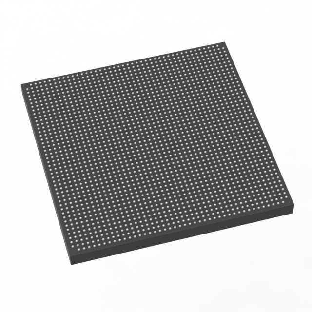
Overview of 5SGXEABN3F45C3G – Stratix V GX FPGA, 952,000 logic elements, 840 I/O, 1932-BBGA
The 5SGXEABN3F45C3G is a Stratix® V GX field programmable gate array (FPGA) from Intel, offered in a 1932-ball FCBGA package. This commercial-grade device delivers a very large logic fabric paired with substantial on-chip memory and a high I/O count, targeting complex digital designs that require dense logic, broad connectivity, and integrated memory resources.
With 952,000 logic elements, approximately 53.25 Mbits of embedded RAM and up to 840 user I/O pins, this device is suited for applications where large-scale programmable logic and extensive I/O routing are required within a surface-mount FCBGA form factor.
Key Features
- Core Logic Capacity — 952,000 logic elements to implement large-scale digital designs and complex logic functions.
- Embedded Memory — Approximately 53.25 Mbits of on-chip RAM for buffering, FIFOs, and local storage to support data-intensive tasks.
- I/O Resources — Up to 840 user I/O pins enabling extensive external interfacing and high connector density for system integration.
- Power Supply — Core supply range from 820 mV to 880 mV, allowing designers to plan power delivery for the FPGA core precisely.
- Package & Mounting — 1932-BBGA FCBGA package (supplier package: 1932-FBGA, FC 45×45) in a surface-mount configuration for standard PCB assembly processes.
- Temperature & Grade — Commercial grade with an operating temperature range of 0 °C to 85 °C for typical commercial-environment deployments.
- RoHS Compliant — Device meets RoHS requirements for restricted substances.
Typical Applications
- High-density digital signal processing — Implement large DSP pipelines and parallel processing architectures using the device’s extensive logic elements and embedded RAM.
- Telecommunications and networking — Support complex packet processing, wide I/O interfacing, and protocol handling leveraging up to 840 user I/O pins.
- Data center acceleration and compute — Deploy custom accelerators and hardware offload engines that require substantial on-chip logic and memory resources.
- Prototype and verification platforms — Use the large programmable fabric to prototype multicore and system-level designs prior to ASIC implementation.
Unique Advantages
- Massive programmable capacity: 952,000 logic elements provide headroom for large, complex designs without partitioning across multiple devices.
- Significant on-chip memory: Approximately 53.25 Mbits of embedded RAM reduces dependence on external memory for many buffering and storage needs.
- High I/O availability: 840 I/O pins simplify interface routing and enable direct connections to numerous peripherals and front-end modules.
- Compact FCBGA packaging: 1932-ball FCBGA offers a high-density, surface-mount solution suitable for space-constrained PCBs while supporting substantial I/O and routing.
- Commercial operating range: Rated for 0 °C to 85 °C, aligning the device with a broad set of standard commercial deployments.
- Standards-conscious supply: RoHS compliance supports environmental and materials planning for product builds.
Why Choose 5SGXEABN3F45C3G?
The 5SGXEABN3F45C3G combines nearly one million logic elements, large embedded memory, and extensive I/O in a single Stratix V GX FCBGA package—providing a consolidated platform for implementing large-scale programmable systems. Its commercial-grade rating and defined core voltage range make it suitable for demanding commercial electronics where predictable electrical and thermal planning is required.
This device is well-suited for engineering teams and system architects building high-capacity FPGA-based solutions that need dense logic, substantial on-chip memory, and broad interfacing options while retaining the benefits of a surface-mount FCBGA package and RoHS compliance.
Request a quote or submit a purchasing inquiry to evaluate availability, lead times, and volume pricing for the 5SGXEABN3F45C3G. Our team can provide additional technical documentation and ordering information to support your design and procurement process.


Date Founded: 1968
Headquarters: Santa Clara, California, USA
Employees: 130,000+
Revenue: $54.23 Billion
Certifications and Memberships: ISO9001:2015, ISO14001:2015, ISO17025:2017, ISO27001:2022, ISO45001:2018, ISO50001:2018


