
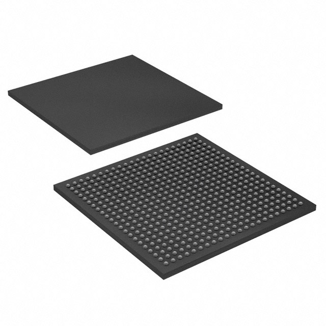
EP2C15AF484I8N
| Part Description |
Cyclone® II Field Programmable Gate Array (FPGA) IC 315 239616 14448 484-BGA |
|---|---|
| Quantity | 208 Available (as of June 10, 2026) |

| Product Category | Field Programmable Gate Array (FPGA) |
|---|---|
| Manufacturer | Intel |
| Manufacturing Status | Active |
| Manufacturer Standard Lead Time | 26 Weeks |
| Datasheet |
Specifications & Environmental
| Device Package | 484-FBGA (23x23) | Grade | Industrial | Operating Temperature | -40°C – 100°C | ||
|---|---|---|---|---|---|---|---|
| Package / Case | 484-BGA | Number of I/O | 315 | Voltage | 1.15 V - 1.25 V | ||
| Mounting Method | Surface Mount | RoHS Compliance | RoHS Compliant | REACH Compliance | REACH Unaffected | ||
| Moisture Sensitivity Level | 3 (168 Hours) | Number of LABs/CLBs | 903 | Number of Logic Elements/Cells | 14448 | ||
| Number of Gates | N/A | ECCN | 3A991D | HTS Code | 8542.39.0001 | ||
| Qualification | N/A | Total RAM Bits | 239616 |
Overview of EP2C15AF484I8N – Cyclone® II Field Programmable Gate Array (FPGA) IC 315 239616 14448 484-BGA
The EP2C15AF484I8N is an Intel Cyclone® II FPGA in a 484-ball BGA package, offered in an industrial-grade temperature range. It combines 14,448 logic elements with a flexible I/O fabric and on-chip resources targeted at low-cost embedded processing and DSP-oriented applications.
Designed for systems that require moderate logic density, substantial I/O count, and low-voltage operation, this device addresses industrial control, embedded acceleration, and interface-bridging use cases while supporting standard FPGA configuration and clocking features.
Key Features
- Logic Capacity — 14,448 logic elements for implementing glue logic, state machines, and mid-sized custom accelerators.
- Embedded Memory — Approximately 0.24 Mbits of on-chip RAM (239,616 bits) to support FIFOs, small buffers, and local storage without external memory.
- I/O Resources — 315 user I/Os to support wide parallel interfaces, multiple peripherals, and external memory connections.
- Power and Voltage — Core supply range of 1.15 V to 1.25 V to match system power rails and enable low-voltage operation.
- Industrial Temperature Grade — Specified for operation from −40 °C to 100 °C for demanding environments.
- Package and Mounting — 484-BGA package (supplier device package: 484-FBGA, 23×23) with surface-mount construction for compact board integration.
- Clocking and DSP-Friendly Blocks — Device family features global clock networks, PLLs, and embedded multipliers to support synchronous designs and DSP tasks.
- I/O and Interface Features — Architecture documentation references advanced I/O capabilities such as programmable drive strength, series on-chip termination, differential interfaces, and multi-voltage I/O bank support.
- Configuration & Test — JTAG boundary-scan support and a variety of configuration schemes are documented for device programming and system test.
- Compliance — RoHS compliant.
Typical Applications
- Embedded Processing — Implement microcontroller peripherals, custom accelerators, and control logic using the device’s logic elements and on-chip RAM.
- DSP and Signal Processing — Use embedded multipliers and synchronous clocking resources for low-cost DSP functions and data-path acceleration.
- Industrial Control & Automation — Leverage the industrial temperature range and extensive I/O to interface sensors, actuators, and fieldbus peripherals.
- Interface Bridging & Protocol Conversion — Large I/O count and configurable I/O standards support protocol translation and external memory interfacing tasks.
Unique Advantages
- Balanced Logic and Memory — 14,448 logic elements combined with approximately 0.24 Mbits of embedded RAM enable compact implementations of control and buffering functions without external SRAM.
- High I/O Density — 315 I/Os allow broad peripheral connectivity and parallel bus support, reducing the need for external interface components.
- Industrial Reliability — Specified operation from −40 °C to 100 °C supports deployment in temperature-challenging environments.
- Compact Package — 484-BGA (23×23) surface-mount package helps save PCB area while providing the signal density required for complex I/O routing.
- Low-Voltage Core — 1.15 V to 1.25 V core supply range aligns with modern low-voltage power domains for efficient system design.
- Integrated Clocking and DSP Resources — Documented global clock networks, PLLs, and embedded multipliers simplify timing architectures and accelerate DSP workloads.
Why Choose EP2C15AF484I8N?
The EP2C15AF484I8N places a practical mix of logic capacity, on-chip memory, and a high I/O count into an industrial-grade Cyclone II package. It is suited to designers needing a mid-range FPGA option for embedded processing, interface bridging, and DSP-lean implementations where temperature resilience and compact packaging matter.
Backed by documented family-level features such as programmable I/O, clock management, and standard configuration and test mechanisms, this device provides a clear upgrade path within the Cyclone II device family while delivering predictable integration into industrial and embedded systems.
Request a quote or submit a sales inquiry to evaluate EP2C15AF484I8N for your next design project.


Date Founded: 1968
Headquarters: Santa Clara, California, USA
Employees: 130,000+
Revenue: $54.23 Billion
Certifications and Memberships: ISO9001:2015, ISO14001:2015, ISO17025:2017, ISO27001:2022, ISO45001:2018, ISO50001:2018


