
EP3SE260H780C3N
| Part Description |
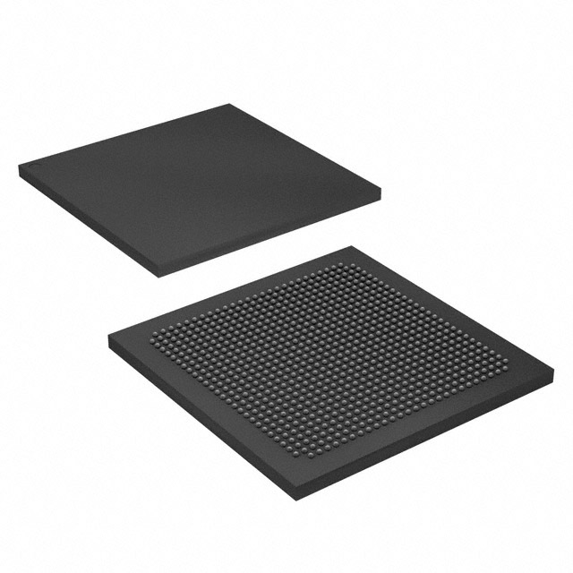
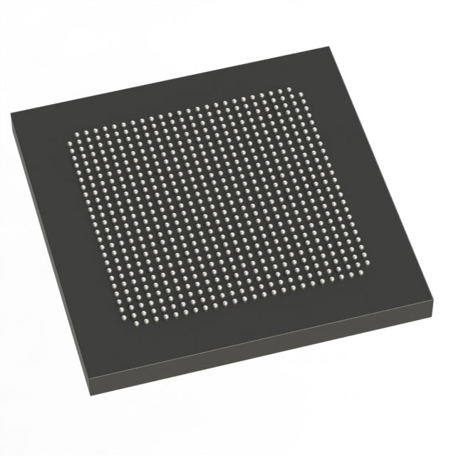
Stratix® III E Field Programmable Gate Array (FPGA) IC 488 16672768 255000 780-BBGA, FCBGA |
|---|---|
| Quantity | 859 Available (as of June 10, 2026) |

| Product Category | Field Programmable Gate Array (FPGA) |
|---|---|
| Manufacturer | Intel |
| Manufacturing Status | Obsolete |
| Manufacturer Standard Lead Time | Contact Us |
| Datasheet |
Specifications & Environmental
| Device Package | 780-HBGA (33x33) | Grade | Commercial | Operating Temperature | 0°C – 85°C | ||
|---|---|---|---|---|---|---|---|
| Package / Case | 780-BBGA, FCBGA | Number of I/O | 488 | Voltage | 860 mV - 1.15 V | ||
| Mounting Method | Surface Mount | RoHS Compliance | RoHS Compliant | REACH Compliance | REACH Unknown | ||
| Moisture Sensitivity Level | 3 (168 Hours) | Number of LABs/CLBs | 10200 | Number of Logic Elements/Cells | 255000 | ||
| Number of Gates | N/A | ECCN | 3A001A7A | HTS Code | 8542.39.0001 | ||
| Qualification | N/A | Total RAM Bits | 16672768 |
Overview of EP3SE260H780C3N – Stratix® III FPGA, 780-BBGA
The EP3SE260H780C3N is a Stratix® III field-programmable gate array (FPGA) in a 780-BBGA (FCBGA) package, offered as a commercial‑grade, surface‑mount device. It integrates a high density of programmable logic, embedded memory, DSP resources and advanced I/O architecture from the Stratix III device family to address demanding system and board-level functions.
Designed for applications requiring substantial on‑chip logic and memory resources, this device delivers a combination of programmable logic capacity, approximately 16.67 Mbits of embedded memory, and 488 general I/O pins while operating across a VCC range of 860 mV to 1.15 V and a commercial temperature range of 0 °C to 85 °C.
Key Features
- High Logic Capacity — 255,000 logic elements (cells) provides extensive programmable fabric for complex logic, control and data‑path implementations.
- Embedded Memory — Approximately 16.67 Mbits of on‑chip RAM (TriMatrix embedded memory blocks referenced in the Stratix III documentation) to support buffering, FIFOs and on‑chip data storage.
- DSP and Arithmetic Resources — Stratix III family DSP blocks and arithmetic resources (documented in the device handbook) for high‑throughput signal processing and computational tasks.
- Rich I/O — 488 I/O pins and documented high‑speed differential I/O interfaces with DPA support for demanding serial and parallel connectivity.
- Clocking and PLLs — Integrated clock networks and PLL resources (described in the Stratix III handbook) for flexible clock management and domain crossing.
- Configuration and Test — Standard configuration and IEEE 1149.1 (JTAG) boundary‑scan testing support as described in the device documentation for system bring‑up and board test.
- Design Security and Reliability — Device handbook references design security features and SEU mitigation options to support protected and resilient designs.
- Package & Mounting — 780‑BBGA (FCBGA) package; supplier device package listed as 780‑HBGA (33×33). Surface mount mounting type simplifies board assembly for compact, high‑density designs.
- Power and Temperature — Core voltage range specified at 860 mV to 1.15 V and an operating temperature range of 0 °C to 85 °C (commercial grade).
- RoHS Compliant — Device meets RoHS environmental requirements.
Typical Applications
- High‑Speed Interfaces — Implement protocol bridging and interface logic that leverage the device's high I/O count and documented high‑speed differential I/O capabilities.
- Signal Processing & DSP — Use the Stratix III DSP resources and large logic capacity for real‑time filtering, modulation/demodulation, and other compute‑intensive algorithms.
- Memory Controller & Buffering — On‑chip memory (approximately 16.67 Mbits) and abundant logic support custom external memory interfaces and on‑chip buffering.
- System Integration & Prototyping — High logic density and flexible clocking make the device suitable for integrating multiple functions and validating complex system architectures.
Unique Advantages
- High density programmable fabric: 255,000 logic elements enable consolidation of multiple subsystems into a single FPGA, reducing board complexity and part count.
- Substantial embedded memory: Approximately 16.67 Mbits of on‑chip RAM reduces reliance on external memory for many buffering and packet‑storage tasks.
- Extensive I/O capability: 488 I/O pins and documented high‑speed I/O architectures support broad connectivity requirements without additional I/O expanders.
- Family‑level feature set: Stratix III architecture elements such as DSP blocks, PLLs, and advanced interconnects provide proven building blocks for performance‑oriented designs.
- Commercial availability and RoHS compliance: Commercial grade rating and RoHS compliance support mainstream product development and regulatory needs.
- Surface‑mount 780‑BBGA package: Compact FCBGA implementation aids in space‑constrained board layouts while providing thermal and electrical packaging suitable for high‑density designs.
Why Choose EP3SE260H780C3N?
The EP3SE260H780C3N delivers a high‑density Stratix III FPGA option for designs that require substantial logic resources, significant embedded memory, and broad I/O capability in a commercial‑grade, surface‑mount 780‑BBGA package. Its combination of programmable logic, DSP resources and documented family features such as TriMatrix memory, clock networks and high‑speed I/O make it well suited for systems that integrate complex signal processing, interface logic and memory controller functions.
Choose this device for projects that demand scalability within the Stratix III family, a sizable on‑chip resource set, and documented configuration, test and reliability features to support robust product development and deployment.
If you would like pricing, availability, or a formal quote for EP3SE260H780C3N, please submit a request for a quote or pricing inquiry and our team will respond with the next steps.


Date Founded: 1968
Headquarters: Santa Clara, California, USA
Employees: 130,000+
Revenue: $54.23 Billion
Certifications and Memberships: ISO9001:2015, ISO14001:2015, ISO17025:2017, ISO27001:2022, ISO45001:2018, ISO50001:2018


