
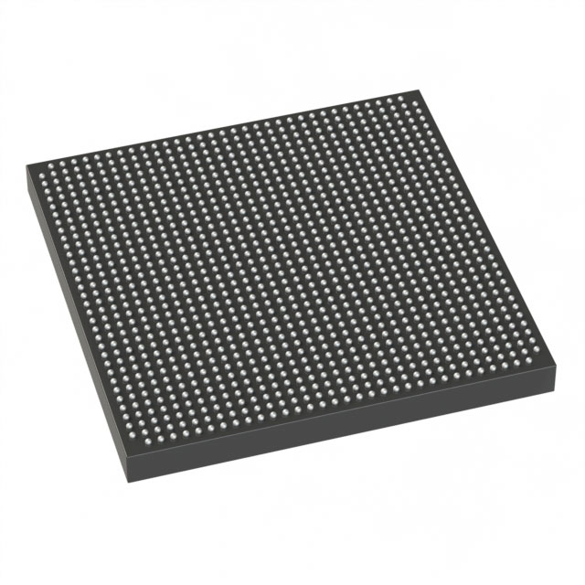
EP3SL110F1152C2N
| Part Description |
Stratix® III L Field Programmable Gate Array (FPGA) IC 744 4992000 107500 1152-BBGA, FCBGA |
|---|---|
| Quantity | 102 Available (as of June 10, 2026) |

| Product Category | Field Programmable Gate Array (FPGA) |
|---|---|
| Manufacturer | Intel |
| Manufacturing Status | Obsolete |
| Manufacturer Standard Lead Time | Contact Us |
| Datasheet |
Specifications & Environmental
| Device Package | 1152-FBGA (35x35) | Grade | Commercial | Operating Temperature | 0°C – 85°C | ||
|---|---|---|---|---|---|---|---|
| Package / Case | 1152-BBGA, FCBGA | Number of I/O | 744 | Voltage | 860 mV - 1.15 V | ||
| Mounting Method | Surface Mount | RoHS Compliance | RoHS Compliant | REACH Compliance | REACH Unknown | ||
| Moisture Sensitivity Level | 3 (168 Hours) | Number of LABs/CLBs | 4300 | Number of Logic Elements/Cells | 107500 | ||
| Number of Gates | N/A | ECCN | 3A001A2C | HTS Code | 8542.39.0001 | ||
| Qualification | N/A | Total RAM Bits | 4992000 |
Overview of EP3SL110F1152C2N – Stratix® III L FPGA, 1152‑FBGA, 107,500 Logic Elements
The EP3SL110F1152C2N is a Stratix® III L Field Programmable Gate Array (FPGA) IC from Intel offered in a 1152‑FBGA (35 × 35) package. It delivers a high count of configurable logic resources, abundant embedded RAM, and a large I/O complement for dense, system‑level FPGA implementations. Targeted at commercial‑grade designs, it provides designers with a compact, surface‑mount FPGA option for applications requiring significant logic, memory, and I/O integration.
Key Features
- Core Logic Provides 107,500 logic elements to implement complex digital functions and custom logic architectures.
- Embedded Memory Approximately 4.992 Mbits of on‑chip RAM to support buffers, FIFOs, and local data storage for high‑throughput logic.
- I/O Density Up to 744 I/O pins to support broad peripheral interfacing and multi‑channel connectivity within a single device.
- Power Operates from a core voltage supply range of 860 mV to 1.15 V to match system power rails and design requirements.
- Package & Mounting Available in a 1152‑FBGA surface‑mount package (35 × 35 mm) for high‑density board layouts and scalable assembly processes.
- Operating Range & Grade Commercial grade device with an operating temperature range of 0 °C to 85 °C and RoHS compliance for regulatory alignment.
Typical Applications
- Data and Control Interfaces High I/O count supports board‑level interface consolidation and multi‑channel signal routing.
- Compute and Acceleration Large logic element count and embedded RAM enable custom datapath and accelerator implementations.
- System Integration Compact FBGA package and surface‑mount mounting simplify integration into dense, space‑constrained designs.
- Prototyping and Custom Logic Flexible logic resources allow rapid implementation of custom functions and proof‑of‑concept designs.
Unique Advantages
- High Logic Capacity: 107,500 logic elements allow implementation of large, complex digital designs without external logic expansion.
- Substantial On‑Chip Memory: Approximately 4.992 Mbits of embedded RAM reduces dependence on external memory for many buffering and storage needs.
- Extensive I/O Resources: 744 I/O pins provide headroom for multi‑channel interfaces and high peripheral counts within a single device.
- Compact, Manufacturable Package: 1152‑FBGA (35 × 35) surface‑mount package supports high‑density PCB designs and standard assembly flows.
- Commercial‑Grade Reliability: Specified for 0 °C to 85 °C operation and RoHS compliance for deployment in commercial products.
- Flexible Power Interface: Core voltage range of 860 mV to 1.15 V enables compatibility with modern power distributions and optimized power planning.
Why Choose EP3SL110F1152C2N?
The EP3SL110F1152C2N is positioned for designers who require a high‑capacity, high‑I/O FPGA in a compact, surface‑mount form factor. With more than 100k logic elements, nearly 5 Mbits of embedded RAM, and 744 I/Os, it supports integration of complex logic, buffering, and interfacing tasks into a single device while maintaining commercial‑grade operating limits.
This device is suited to engineering teams building dense, performance‑oriented FPGA solutions where board real estate, I/O count, and on‑chip memory are critical considerations. Its combination of resources offers long‑term design scalability and reduced system component count for many commercial applications.
Request a quote or submit a pricing inquiry to learn about availability, lead times, and volume options for the EP3SL110F1152C2N. Our team can provide a tailored quote to support your project timeline and procurement needs.


Date Founded: 1968
Headquarters: Santa Clara, California, USA
Employees: 130,000+
Revenue: $54.23 Billion
Certifications and Memberships: ISO9001:2015, ISO14001:2015, ISO17025:2017, ISO27001:2022, ISO45001:2018, ISO50001:2018


