
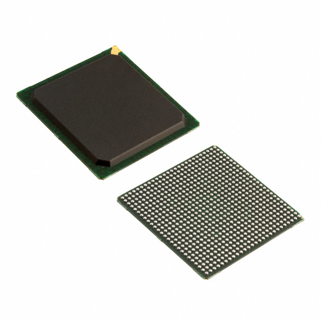
XC2VP50-5FF1517C
| Part Description |
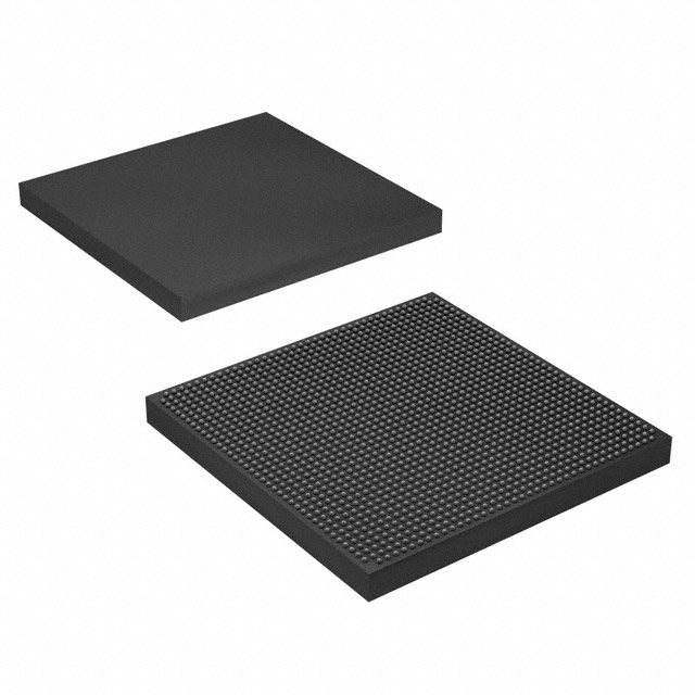
Virtex®-II Pro Field Programmable Gate Array (FPGA) IC 852 4276224 53136 1517-BBGA, FCBGA |
|---|---|
| Quantity | 1,694 Available (as of October 8, 2026) |
| Product Category | Field Programmable Gate Array (FPGA) |
|---|---|
| Manufacturer | AMD |
| Manufacturing Status | Obsolete |
| Manufacturer Standard Lead Time | Contact Us |
| Datasheet |
Specifications & Environmental
| Device Package | 1517-FCBGA (40x40) | Grade | Commercial | Operating Temperature | 0°C – 85°C | ||
|---|---|---|---|---|---|---|---|
| Package / Case | 1517-BBGA, FCBGA | Number of I/O | 852 | Voltage | 1.425 V - 1.575 V | ||
| Mounting Method | Surface Mount | RoHS Compliance | RoHS non-compliant | REACH Compliance | REACH Unaffected | ||
| Moisture Sensitivity Level | 4 (72 Hours) | Number of LABs/CLBs | 5904 | Number of Logic Elements/Cells | 53136 | ||
| Number of Gates | N/A | ECCN | 3A001A7A | HTS Code | 8542.39.0001 | ||
| Qualification | N/A | Total RAM Bits | 4276224 |
Overview of XC2VP50-5FF1517C – Virtex®-II Pro FPGA, 1517-FCBGA
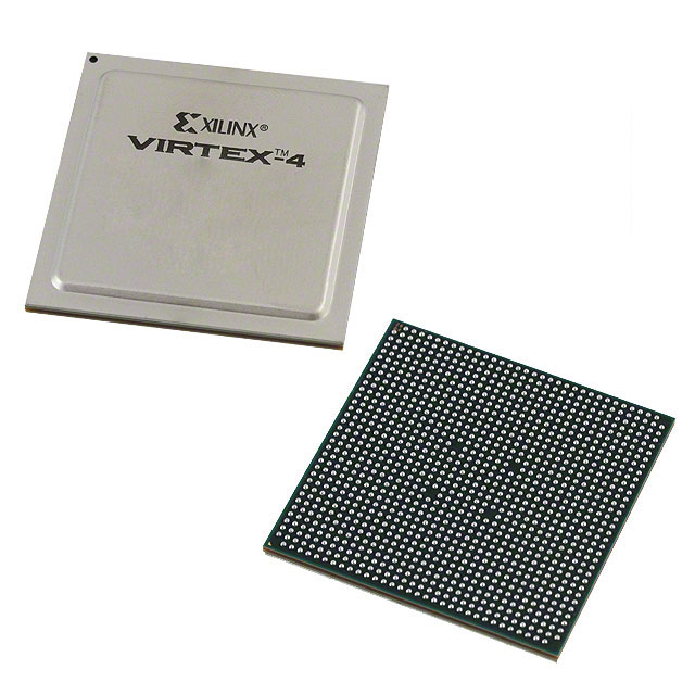
The XC2VP50-5FF1517C is a Virtex®-II Pro Field Programmable Gate Array (FPGA) in a 1517‑ball flip‑chip BGA (FCBGA) package. It combines a high-density logic fabric with embedded memory and I/O resources to support complex, configurable digital systems in commercial applications.
Built on the Virtex‑II Pro family architecture, the device is suitable for designs that require substantial logic and memory capacity alongside advanced I/O. Family-level features include embedded multi‑gigabit transceivers and on‑chip processor block support, providing flexibility for communications and embedded processing applications.
Key Features
- Logic Capacity — 5,904 CLBs providing 53,136 logic cells for implementing complex custom logic and state machines.
- Embedded Memory — Approximately 4.28 Mbits of on‑chip RAM to support buffering, packet processing, and local data storage.
- High I/O Count — Up to 852 user I/O pins available in the 1517‑ball FCBGA package for dense board-level connectivity.
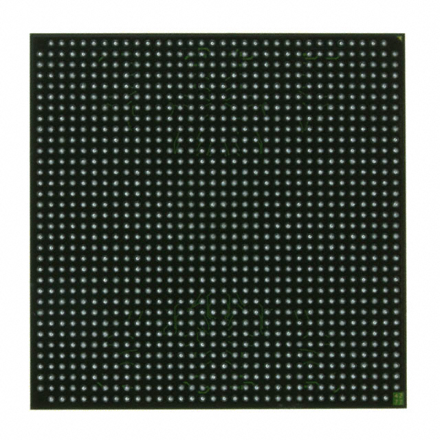
- Device Package & Mounting — 1517‑BBGA (1517‑FCBGA, 40×40) surface‑mount package optimized for high‑pin‑count system designs.
- Power Supply — Core voltage range 1.425 V to 1.575 V to match board power domains and regulator selection.
- Commercial Grade Operating Range — Specified for 0 °C to 85 °C operation for general commercial applications.
- Virtex‑II Pro Family Features — Family‑level capabilities include RocketIO™ multi‑gigabit transceivers, on‑chip PowerPC™ processor block support, dedicated 18×18 multiplier blocks, SelectRAM™ memory hierarchy, and advanced clock management circuitry.
- Standards & Compliance — RoHS compliant for alignment with common environmental requirements.
Typical Applications
- Communications & Networking — Implements protocol processing, packet buffering and high‑density I/O for switches, routers and line cards.
- Embedded Processing — Supports designs that combine FPGA fabric with on‑chip processor blocks for system‑on‑chip architectures and control tasks.
- High‑Speed Serial Interfaces — Enables multi‑gigabit serial link implementation using family RocketIO transceiver capabilities for backplane and board‑to‑board links.
- Custom Logic & Signal Processing — Leverages abundant logic cells, dedicated multipliers, and embedded RAM for DSP, protocol acceleration, and data path functions.
Unique Advantages
- High integration density: Combines 53,136 logic cells and approximately 4.28 Mbits of embedded RAM in a single 1517‑ball FCBGA package, reducing board area and component count.
- Large I/O footprint: 852 I/Os support complex interfacing needs without additional I/O expanders or multiplexing.
- Family-level serial and processing support: Virtex‑II Pro family features like RocketIO and on‑chip processor blocks enable mixed computation and high‑speed connectivity in one device.
- Commercial temperature rating: Specified for 0 °C to 85 °C operation to match mainstream commercial product deployment requirements.
- RoHS compliance: Meets common environmental substance restrictions for streamlined regulatory alignment.
Why Choose XC2VP50-5FF1517C?
The XC2VP50-5FF1517C positions itself for commercial designs that demand substantial programmable logic, significant embedded memory, and a very large I/O complement within a single FPGA package. Its Virtex‑II Pro family capabilities provide designers with the architectural building blocks for communication, embedded processing and signal‑processing applications while simplifying system integration.
For engineering teams developing complex, board‑level systems, this device offers the scalability and integration to reduce BOM complexity and accelerate time‑to‑market, with the vendor ecosystem and datasheet guidance to support implementation and verification.
Request a quote or submit a procurement inquiry to get pricing and availability for XC2VP50-5FF1517C.
























Date Founded: 1969
Headquarters: Santa Clara, California, USA
Employees: 25,000+
Revenue: $22.68 Billion
Certifications and Memberships: ISO9001:2015, RoHS, REACH











