
XC3S4000-5FG676C
| Part Description |
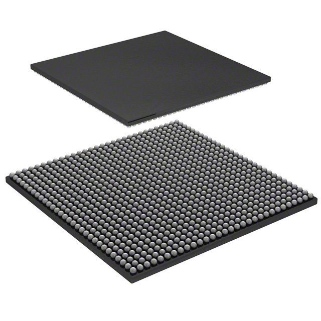
Spartan®-3 Field Programmable Gate Array (FPGA) IC 489 1769472 62208 676-BGA |
|---|---|
| Quantity | 250 Available (as of October 8, 2026) |

| Product Category | Field Programmable Gate Array (FPGA) |
|---|---|
| Manufacturer | AMD |
| Manufacturing Status | Last Time Buy |
| Manufacturer Standard Lead Time | 12 Weeks |
| Datasheet |
Specifications & Environmental
| Device Package | 676-FBGA (27x27) | Grade | Commercial | Operating Temperature | 0°C – 85°C | ||
|---|---|---|---|---|---|---|---|
| Package / Case | 676-BGA | Number of I/O | 489 | Voltage | 1.14 V - 1.26 V | ||
| Mounting Method | Surface Mount | RoHS Compliance | RoHS non-compliant | REACH Compliance | REACH Unaffected | ||
| Moisture Sensitivity Level | 3 (168 Hours) | Number of LABs/CLBs | 6912 | Number of Logic Elements/Cells | 62208 | ||
| Number of Gates | 4000000 | ECCN | 3A991D | HTS Code | 8542.39.0001 | ||
| Qualification | N/A | Total RAM Bits | 1769472 |
Overview of XC3S4000-5FG676C – Spartan®-3 FPGA, 676-BGA
The XC3S4000-5FG676C is a Spartan®-3 Field Programmable Gate Array (FPGA) IC from AMD designed for commercial applications. It delivers a high-density programmable fabric with 6,912 configuration logic blocks (CLBs) and 62,208 logic elements, alongside approximately 1.77 Mbits of embedded memory and 489 user I/O pins to support complex digital designs.
Packaged in a 676-ball fine-pitch BGA (27 × 27 mm) and specified for a core voltage range of 1.14 V to 1.26 V with an operating temperature range of 0 °C to 85 °C, this device targets designs that require substantial logic density, on-chip RAM, and large I/O counts in a compact surface-mount form factor.
Key Features
- Core Architecture Spartan®-3 FPGA fabric with 6,912 CLBs enabling synchronous, user-defined digital logic implementations.
- Logic Capacity 62,208 logic elements and approximately 4,000,000 gates for high-density combinational and sequential logic integration.
- Embedded Memory Approximately 1.77 Mbits of on-chip RAM to support buffers, FIFOs, and local data storage without external memory.
- I/O Resources 489 user I/O pins to interface with peripherals, sensors, or system-level buses while minimizing external routing complexity.
- Package & Mounting 676-FBGA package (27 × 27 mm), surface-mount mounting type, providing a compact, board-friendly footprint for dense designs.
- Power Core voltage specified from 1.14 V to 1.26 V, allowing precise power planning for the FPGA core domain.
- Operating Range & Grade Commercial grade operation from 0 °C to 85 °C suitable for standard consumer and industrial-facing commercial products.
- RoHS Compliance Device is compliant with RoHS standards for lead-free assembly and environmental regulatory requirements.
Typical Applications
- Custom Digital Processing Implement high-density custom logic, state machines, or protocol engines using the device’s large logic element and gate count.
- Embedded Memory-Intensive Designs Use the approximately 1.77 Mbits of on-chip RAM for buffering, packet queues, or small data caches without immediate external memory.
- High-Connectivity Interfaces Drive multiple peripherals or parallel interfaces leveraging 489 user I/O pins to consolidate system connectivity on-chip.
Unique Advantages
- High Logic Density: 62,208 logic elements and 6,912 CLBs enable complex designs to be implemented on a single device, reducing board-level component count.
- Substantial On-Chip RAM: Approximately 1.77 Mbits of embedded memory reduces reliance on external RAM for many control and buffering tasks.
- Extensive I/O Count: 489 I/O pins simplify system integration by accommodating multiple interfaces and peripherals without additional I/O expanders.
- Compact BGA Package: 676-FBGA (27 × 27 mm) provides a balance of pin density and board space efficiency for space-constrained designs.
- Commercial Temperature Qualification: Rated from 0 °C to 85 °C for reliable operation within standard commercial environments.
- RoHS Compliant: Supports lead-free assembly requirements for regulated markets.
Why Choose XC3S4000-5FG676C?
The XC3S4000-5FG676C positions itself as a commercially graded, high-density FPGA choice for designs that require extensive logic resources, on-chip RAM, and a large number of I/O in a compact BGA package. Its combination of 62,208 logic elements, approximately 1.77 Mbits of embedded memory, and 489 I/O pins makes it well suited for developers who need to consolidate functionality onto a single programmable device while managing board space and BOM complexity.
For teams focused on scalable, robust digital designs in commercial applications, this Spartan®-3 device offers a clear, verifiable specification set for power, thermal range, and packaging that supports predictable integration and long-term maintainability.
If you would like pricing, availability, or to request a formal quote for the XC3S4000-5FG676C, please submit a quote request or sales inquiry and our team will respond with details tailored to your project requirements.


























Date Founded: 1969
Headquarters: Santa Clara, California, USA
Employees: 25,000+
Revenue: $22.68 Billion
Certifications and Memberships: ISO9001:2015, RoHS, REACH











