
XC3S400AN-5FTG256C
| Part Description |
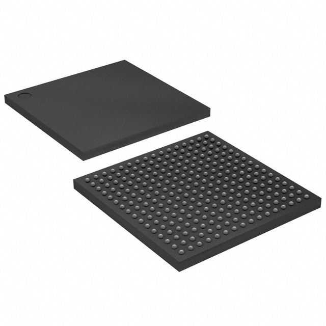
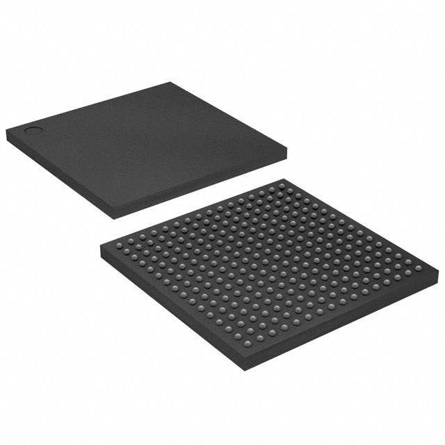
Spartan®-3AN Field Programmable Gate Array (FPGA) IC 195 368640 8064 256-LBGA |
|---|---|
| Quantity | 806 Available (as of October 8, 2026) |
| Product Category | Field Programmable Gate Array (FPGA) |
|---|---|
| Manufacturer | AMD |
| Manufacturing Status | Last Time Buy |
| Manufacturer Standard Lead Time | 12 Weeks |
| Datasheet |
Specifications & Environmental
| Device Package | 256-FTBGA (17x17) | Grade | Commercial | Operating Temperature | 0°C – 85°C | ||
|---|---|---|---|---|---|---|---|
| Package / Case | 256-LBGA | Number of I/O | 195 | Voltage | 1.14 V - 1.26 V | ||
| Mounting Method | Surface Mount | RoHS Compliance | ROHS3 Compliant | REACH Compliance | REACH Unaffected | ||
| Moisture Sensitivity Level | 3 (168 Hours) | Number of LABs/CLBs | 896 | Number of Logic Elements/Cells | 8064 | ||
| Number of Gates | 400000 | ECCN | EAR99 | HTS Code | 8542.39.0001 | ||
| Qualification | N/A | Total RAM Bits | 368640 |
Overview of XC3S400AN-5FTG256C – Spartan®-3AN FPGA, 256‑LBGA
The XC3S400AN-5FTG256C is a Spartan®-3AN field programmable gate array (FPGA) from AMD, supplied in a 256‑pin low‑profile BGA package. It combines configurable logic resources, embedded RAM, and a high count of user I/Os for implementing custom digital functions in compact, surface‑mount designs.
With 8,064 logic elements, approximately 0.369 Mbits of on‑chip RAM and 195 user I/Os, this commercial‑grade device is targeted at applications that require flexible logic integration and significant I/O density while operating within a 1.14 V to 1.26 V core voltage and a 0 °C to 85 °C temperature range.
Key Features
- Logic Capacity 8,064 logic elements for implementing custom digital functions and control logic.
- Embedded Memory Approximately 0.369 Mbits of on‑chip RAM for buffering, small data storage and state machines.
- I/O Resources 195 user I/Os to support multiple parallel interfaces and peripheral connections.
- Gate Equivalent Equivalent to approximately 400,000 gates for mapping complex logic and glue‑logic tasks.
- Power Supply Core voltage operating range of 1.14 V to 1.26 V to match required FPGA core power rails.
- Package and Mounting 256‑LBGA (supplier package: 256‑FTBGA 17×17), surface‑mount package suitable for compact PCB layouts.
- Operating Range Commercial temperature grade, 0 °C to 85 °C, for standard commercial applications.
- Compliance RoHS compliant for environmental and manufacturing conformity.
Typical Applications
- Embedded Control Use the device’s 8,064 logic elements and on‑chip RAM to implement custom control algorithms and state machines in embedded systems.
- Interface Bridging Leverage 195 I/Os to connect and translate between multiple parallel and serial interfaces on a single FPGA.
- Prototyping and Development Suitable for board‑level prototyping where reconfigurable logic and moderate memory capacity accelerate design iteration.
- Data Buffering and Glue Logic On‑chip RAM and gate capacity enable temporary data storage and consolidation of discrete logic functions.
Unique Advantages
- High Logic Integration: 8,064 logic elements provide the capacity to integrate multiple functions and reduce external component count.
- Significant On‑Chip Memory: Approximately 0.369 Mbits of embedded RAM supports buffering and local data handling without added memory devices.
- Ample I/O Count: 195 user I/Os simplify board routing for designs requiring many external signals or parallel interfaces.
- Compact, Surface‑Mount Package: 256‑LBGA (17×17 FTBGA) enables higher density PCB layouts and fits space‑constrained designs.
- Controlled Power Requirements: Narrow core voltage range (1.14 V–1.26 V) simplifies supply design for the FPGA core.
- RoHS Compliant: Conforms to RoHS requirements for environmentally compliant manufacturing.
Why Choose XC3S400AN-5FTG256C?
The XC3S400AN-5FTG256C positions itself as a flexible, commercially graded FPGA option for projects that need moderate logic density, substantial I/O capability, and embedded RAM in a compact surface‑mount package. Its combination of 8,064 logic elements, approximately 0.369 Mbits of on‑chip RAM and 195 I/Os enables consolidation of glue logic, buffering, and interface functions into a single programmable device.
This part suits design teams and procurement looking for a configurable solution that balances integration and board‑level density while operating within standard commercial temperature and core voltage ranges. Its RoHS compliance and common BGA footprint support standard manufacturing flows and assembly processes.
Request a quote or submit an inquiry to purchase the XC3S400AN-5FTG256C and discuss pricing, availability, and lead times with our team.























Date Founded: 1969
Headquarters: Santa Clara, California, USA
Employees: 25,000+
Revenue: $22.68 Billion
Certifications and Memberships: ISO9001:2015, RoHS, REACH











