
XC3S50AN-5FT256C
| Part Description |
Spartan®-3AN Field Programmable Gate Array (FPGA) IC 195 55296 1584 256-LBGA |
|---|---|
| Quantity | 393 Available (as of October 7, 2026) |

| Product Category | Field Programmable Gate Array (FPGA) |
|---|---|
| Manufacturer | AMD |
| Manufacturing Status | Obsolete |
| Manufacturer Standard Lead Time | Contact Us |
| Datasheet |
Specifications & Environmental
| Device Package | 256-FTBGA (17x17) | Grade | Commercial | Operating Temperature | 0°C – 85°C | ||
|---|---|---|---|---|---|---|---|
| Package / Case | 256-LBGA | Number of I/O | 195 | Voltage | 1.14 V - 1.26 V | ||
| Mounting Method | Surface Mount | RoHS Compliance | RoHS non-compliant | REACH Compliance | REACH Unaffected | ||
| Moisture Sensitivity Level | 3 (168 Hours) | Number of LABs/CLBs | 176 | Number of Logic Elements/Cells | 1584 | ||
| Number of Gates | 50000 | ECCN | EAR99 | HTS Code | 8542.39.0001 | ||
| Qualification | N/A | Total RAM Bits | 55296 |
Overview of XC3S50AN-5FT256C – Spartan®-3AN FPGA, 1,584 Logic Elements, 195 I/O, 256-LBGA
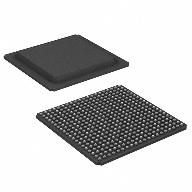
The XC3S50AN-5FT256C is a Spartan®-3AN field programmable gate array (FPGA) IC from AMD, packaged in a 256-ball L-BGA. It delivers a compact programmable-logic solution with 1,584 logic elements and 176 CLBs for designs that require moderate logic capacity and extensive I/O.
Designed for commercial-grade applications, this device offers on-chip memory, flexible I/O count, and low-voltage core operation, making it suitable for a range of embedded and interface-focused implementations that need reprogrammability and integration.
Key Features
- Core Logic 1,584 logic elements and 176 CLBs provide programmable logic resources for glue logic, control functions, and custom digital blocks.
- On-Chip Memory 55,296 bits of embedded RAM support moderate buffering, FIFOs, and small data storage needs on-chip (≈0.055 Mbits).
- I/O Capacity 195 user I/O pins allow broad connectivity to peripherals, interfaces, and external devices in mixed-signal systems.
- Performance Scale Approximately 50,000 equivalent gates enable implementation of moderate-complexity digital functions while keeping board footprint small.
- Power and Voltage Core supply range of 1.14 V to 1.26 V supports low-voltage operation consistent with modern FPGA core domains.
- Package and Mounting 256-LBGA (supplier package: 256-FTBGA, 17×17) in a surface-mount format simplifies integration into compact PCBs.
- Operating Conditions Commercial grade with an operating temperature range of 0 °C to 85 °C and RoHS compliance for lead-free manufacturing workflows.
Typical Applications
- Interface Bridging and Glue Logic Use the XC3S50AN-5FT256C to implement custom protocol adapters and aggregators, leveraging 195 I/O pins for diverse peripheral connections.
- Embedded Control Implement control logic and finite-state machines with the available 1,584 logic elements and 176 CLBs for compact embedded systems.
- On-Board Data Buffering Employ the 55,296 bits of on-chip RAM for buffering, small FIFOs, and temporary data storage without external memory.
- Proof-of-Concept and Prototyping The device’s programmable nature and moderate gate count make it suitable for early-stage development and validation of custom digital functions.
Unique Advantages
- Balanced Logic-to-I/O Ratio: A combination of 1,584 logic elements and 195 I/O pins provides flexibility for designs that need substantial interfacing without excessive logic overhead.
- Compact, Surface-Mount Package: The 256-LBGA footprint (256-FTBGA, 17×17) enables high-density PCB integration while preserving board space.
- On-Chip Memory Availability: 55,296 bits of RAM reduce the need for some external memory, simplifying BOM and board routing for small buffers and FIFOs.
- Low-Voltage Core Operation: A 1.14 V to 1.26 V supply range aligns with low-voltage design domains, supporting efficient core power delivery.
- Commercial-Grade and RoHS Compliant: Rated for 0 °C to 85 °C and compliant with RoHS, suitable for standard commercial production environments.
Why Choose XC3S50AN-5FT256C?
The XC3S50AN-5FT256C positions itself as a compact, commercially graded FPGA for designers who need moderate logic capacity, extensive I/O, and on-chip memory in a small surface-mount package. Its combination of 1,584 logic elements, 195 I/O pins, and 55,296 bits of RAM enables integration of interface logic, control functions, and local buffering without a large board footprint.
This device is well suited to procurement and engineering teams targeting commercial embedded systems, interface bridging, and prototyping efforts where reprogrammability and compact integration are priorities. RoHS compliance and a defined operating range support standard manufacturing and deployment requirements.
Request a quote or submit an inquiry to obtain pricing and availability for the XC3S50AN-5FT256C.

























Date Founded: 1969
Headquarters: Santa Clara, California, USA
Employees: 25,000+
Revenue: $22.68 Billion
Certifications and Memberships: ISO9001:2015, RoHS, REACH











