
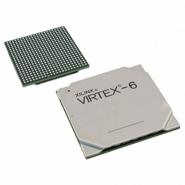
XC6VCX75T-1FFG784C
| Part Description |
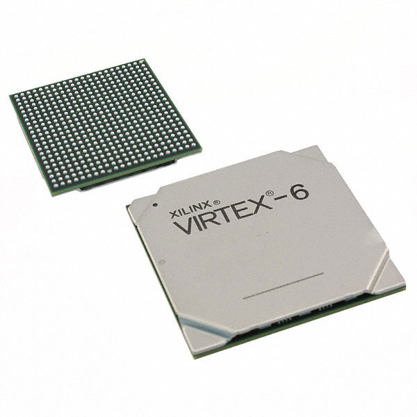
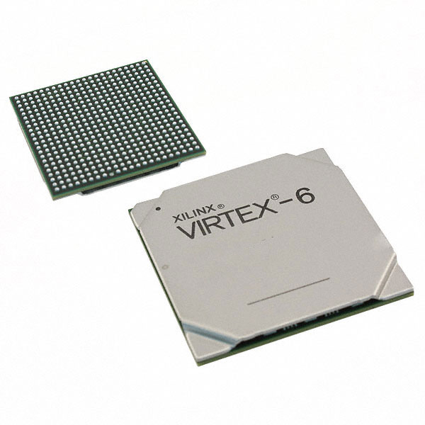
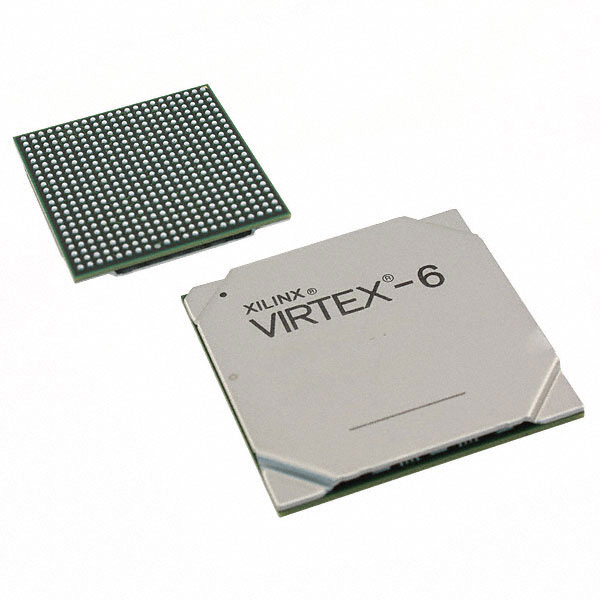
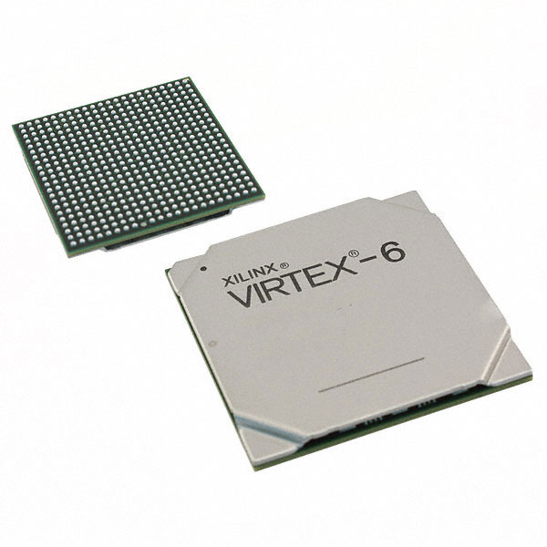
Virtex®-6 CXT Field Programmable Gate Array (FPGA) IC 360 5750784 74496 784-BBGA, FCBGA |
|---|---|
| Quantity | 407 Available (as of October 8, 2026) |
| Product Category | Field Programmable Gate Array (FPGA) |
|---|---|
| Manufacturer | AMD |
| Manufacturing Status | Active |
| Manufacturer Standard Lead Time | 12 Weeks |
| Datasheet |
Specifications & Environmental
| Device Package | 784-FCBGA (29x29) | Grade | Commercial | Operating Temperature | 0°C – 85°C | ||
|---|---|---|---|---|---|---|---|
| Package / Case | 784-BBGA, FCBGA | Number of I/O | 360 | Voltage | 950 mV - 1.05 V | ||
| Mounting Method | Surface Mount | RoHS Compliance | ROHS3 Compliant | REACH Compliance | REACH Unaffected | ||
| Moisture Sensitivity Level | 4 (72 Hours) | Number of LABs/CLBs | 5820 | Number of Logic Elements/Cells | 74496 | ||
| Number of Gates | N/A | ECCN | 3A991D | HTS Code | 8542.39.0001 | ||
| Qualification | N/A | Total RAM Bits | 5750784 |
Overview of XC6VCX75T-1FFG784C – Virtex®-6 CXT Field Programmable Gate Array, 784‑FCBGA
The XC6VCX75T-1FFG784C is a Virtex®-6 CXT class FPGA from AMD designed for applications that require high integration of logic, memory and high-speed serial interfaces. This surface-mount device provides approximately 74,496 logic elements (based on the device's logic cell count) and roughly 5.75 Mbits of embedded memory, making it suitable for compute- and I/O-intensive designs in commercial-temperature environments.
Built on the Virtex-6 CXT architecture, the device targets designs that benefit from integrated transceivers, programmable I/O, and embedded system blocks—enabling performance, integration and flexibility for networking, signal processing and high-speed interface applications.
Key Features
- Logic Capacity — Approximately 74,496 logic elements and 5,820 CLBs provide a substantial fabric for implementing custom logic, state machines and protocol handling.
- Embedded Memory — Total on-chip RAM of 5,750,784 bits (approximately 5.75 Mbits) with the Virtex-6 CXT family architecture that supports 36-Kb block RAM/FIFOs and flexible dual-port configurations.
- High‑Speed Serial — Family-level GTX transceiver support up to 3.75 Gb/s for multi‑Gb/s serial links and SerDes applications, suitable for serial communications and protocol bridging.
- Integrated Interfaces — Series features include integrated PCI Express® (Gen1) blocks and a tri‑mode Ethernet MAC, enabling embedded endpoint and networking functions within the FPGA fabric.
- I/O and SelectIO Technology — 360 I/O pins with SelectIO capabilities and flexible I/O banking to support a range of I/O standards and memory interface topologies.
- Power and Operating Range — Core supply range of 0.95 V to 1.05 V (device core nominally 1.0 V) and commercial operating range from 0 °C to 85 °C, for standard commercial deployments.
- Package — 784-ball FCBGA package (29 × 29 mm) in a surface-mount form factor for dense board-level integration and high signal-integrity routing.
- RoHS Compliant — Meets RoHS environmental requirements.
Typical Applications
- High‑speed communications — Implement multi‑Gb/s serial links and protocol converters using the device’s GTX transceiver capability and rich I/O.
- Networking and infrastructure — Integrate Ethernet MAC functionality and programmable logic for packet processing, switch control and custom networking features.
- Signal processing and DSP — Use the device’s embedded memory and DSP-focused fabric features (from the Virtex‑6 CXT family) for filtering, aggregation and real‑time data processing.
- PCI Express endpoints — Develop Gen1 PCIe endpoint implementations leveraging the integrated PCI Express interface blocks described in the Virtex‑6 CXT feature set.
Unique Advantages
- Substantial logic resources: Approximately 74,496 logic elements and 5,820 CLBs enable complex custom logic and large FPGA designs without external logic expansion.
- Significant embedded memory: About 5.75 Mbits of on‑chip RAM supports buffering, FIFOs and on‑chip data storage to reduce external memory dependence.
- Integrated serial and interface IP: Family-level support for GTX transceivers, PCIe Gen1 blocks and an Ethernet MAC reduces board-level component count and design complexity.
- Flexible I/O count and packaging: 360 I/Os in a 784‑FCBGA (29×29) package provide a high pin-count solution for dense I/O and multi‑lane interfaces.
- Commercial temperature suitability: Rated for 0 °C to 85 °C operation, appropriate for mainstream commercial applications.
- RoHS compliant: Meets environmental compliance requirements for modern electronic assemblies.
Why Choose XC6VCX75T-1FFG784C?
The XC6VCX75T-1FFG784C combines a substantial logic fabric with embedded memory and family-level integrated serial and interface blocks to support designs that need a balance of compute, memory and high-speed I/O. Its 784‑ball FCBGA package and 360 I/Os make it a compact, board-friendly option for commercial projects that require dense routing and multi‑lane interfaces.
This device is well suited to engineering teams building networking gear, communication endpoints, or signal-processing platforms that can leverage the Virtex‑6 CXT family’s system-level features and the specific resource counts provided for this part. The combination of on-chip memory, logic capacity and integrated IP components offers a path to reduce external components and accelerate system integration.
Request a quote or submit an inquiry to get pricing and availability for XC6VCX75T-1FFG784C and to discuss how this device fits your next FPGA-based design.





















Date Founded: 1969
Headquarters: Santa Clara, California, USA
Employees: 25,000+
Revenue: $22.68 Billion
Certifications and Memberships: ISO9001:2015, RoHS, REACH











