
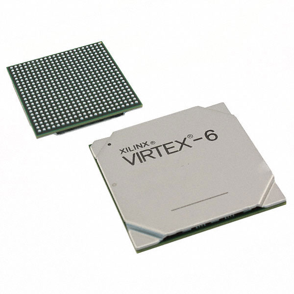
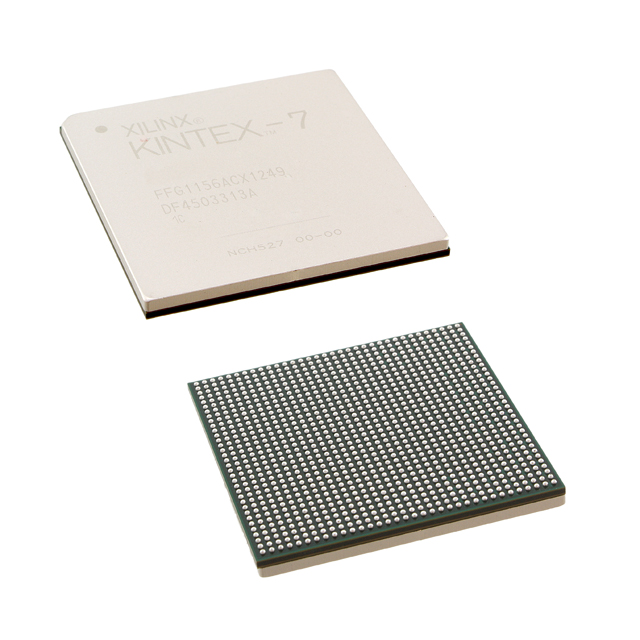
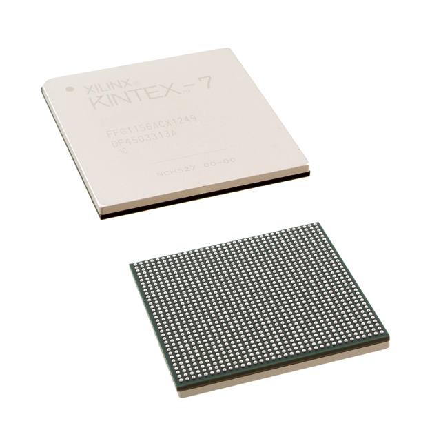
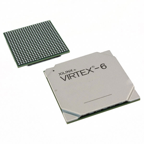
XC6VLX550T-1FFG1759I
| Part Description |
Virtex®-6 LXT Field Programmable Gate Array (FPGA) IC 840 23298048 549888 1759-BBGA, FCBGA |
|---|---|
| Quantity | 770 Available (as of October 8, 2026) |

| Product Category | Field Programmable Gate Array (FPGA) |
|---|---|
| Manufacturer | AMD |
| Manufacturing Status | Active |
| Manufacturer Standard Lead Time | 12 Weeks |
| Datasheet |
Specifications & Environmental
| Device Package | 1759-FCBGA (42.5x42.5) | Grade | Industrial | Operating Temperature | -40°C – 100°C | ||
|---|---|---|---|---|---|---|---|
| Package / Case | 1759-BBGA, FCBGA | Number of I/O | 840 | Voltage | 950 mV - 1.05 V | ||
| Mounting Method | Surface Mount | RoHS Compliance | ROHS3 Compliant | REACH Compliance | REACH Unaffected | ||
| Moisture Sensitivity Level | 4 (72 Hours) | Number of LABs/CLBs | 42960 | Number of Logic Elements/Cells | 549888 | ||
| Number of Gates | N/A | ECCN | 3A001A7A | HTS Code | 8542.39.0001 | ||
| Qualification | N/A | Total RAM Bits | 23298048 |
Overview of XC6VLX550T-1FFG1759I – Virtex®-6 LXT FPGA, 1759-FCBGA (42.5×42.5), Industrial
The XC6VLX550T-1FFG1759I is a Virtex®-6 LXT field programmable gate array (FPGA) IC from AMD, supplied in a 1759-FCBGA package. It targets designs that require very large logic capacity, substantial on-chip RAM, and a high count of general-purpose I/O.
This device is offered in an industrial-grade temperature range and supports a core supply window of 950 mV to 1.05 V, enabling use in systems that must operate across a wide thermal range while maintaining dense digital integration.
Key Features
- Core Architecture Virtex®-6 LXT FPGA architecture provided in the XC6VLX550T-1FFG1759I part.
- Logic Resources 549,888 logic elements to implement large, complex digital designs.
- Embedded Memory Approximately 23.3 Mbits of on-chip RAM for buffering, FIFO structures, and memory-intensive algorithms.
- I/O and Package Up to 840 I/O pins delivered from a 1759-FCBGA (42.5×42.5 mm) package, optimized for high-pin-count system interfaces and board-level routing.
- Power Supply Core voltage support from 950 mV to 1.05 V to match system power delivery requirements.
- Temperature and Grade Industrial-grade device specified for operation from -40°C to 100°C.
- Mounting and Compliance Surface-mount FCBGA package construction; RoHS compliant.
Typical Applications
- Industrial Control and Automation Use the device where wide operating temperatures and large logic resources are required for control, sequencing, and system orchestration.
- High-Density Digital Processing Implement complex logic networks and algorithm acceleration that benefit from nearly 550k logic elements and significant embedded RAM.
- I/O-Intensive Systems Support multi-channel interfaces, parallel buses, and aggregated signal processing with up to 840 I/O pins.
- Data Acquisition and Signal Conditioning Leverage on-chip memory and logic resources for real-time data buffering and preprocessing in measurement and acquisition systems.
Unique Advantages
- Very High Logic Capacity: 549,888 logic elements enable large-scale integration of digital functions on a single device, reducing the need for multiple FPGAs.
- Substantial On-Chip Memory: Approximately 23.3 Mbits of embedded RAM provide local storage for buffering and intermediate data processing, simplifying system memory architecture.
- Extensive I/O Count: 840 I/O pins in a single FCBGA package support dense external interfacing and reduce board-level component count.
- Industrial Temperature Range: Rated from -40°C to 100°C for deployment in temperature-challenging environments.
- Compact, High-Pin-Count Package: The 1759-FCBGA (42.5×42.5 mm) package delivers high pin density in a surface-mount form factor for space-constrained boards.
- RoHS Compliant: Meets RoHS requirements for environmental compliance in assembly and production.
Why Choose XC6VLX550T-1FFG1759I?
The XC6VLX550T-1FFG1759I positions itself for designs that demand very high logic density, significant embedded memory, and a large number of I/O connections within a packaged industrial-grade FPGA. Its combination of nearly 550k logic elements, approximately 23.3 Mbits of on-chip RAM, and 840 I/O pins makes it suitable for consolidated digital systems that prioritize integration and board-level simplicity.
This part is appropriate for engineers and procurement teams specifying FPGAs for industrial applications where operating temperature range, package density, and verified electrical supply windows are important selection criteria.
Request a quote or submit your requirements now to obtain pricing and availability for the XC6VLX550T-1FFG1759I. Include quantity and delivery timing to receive an accurate response.

























Date Founded: 1969
Headquarters: Santa Clara, California, USA
Employees: 25,000+
Revenue: $22.68 Billion
Certifications and Memberships: ISO9001:2015, RoHS, REACH











