
XC6VSX315T-2FFG1759C
| Part Description |
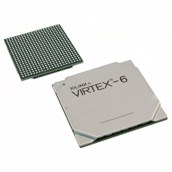
Virtex®-6 SXT Field Programmable Gate Array (FPGA) IC 720 25952256 314880 1759-BBGA, FCBGA |
|---|---|
| Quantity | 191 Available (as of June 10, 2026) |

| Product Category | Field Programmable Gate Array (FPGA) |
|---|---|
| Manufacturer | AMD |
| Manufacturing Status | Active |
| Manufacturer Standard Lead Time | 12 Weeks |
| Datasheet |
Specifications & Environmental
| Device Package | 1759-FCBGA (42.5x42.5) | Grade | Commercial | Operating Temperature | 0°C – 85°C | ||
|---|---|---|---|---|---|---|---|
| Package / Case | 1759-BBGA, FCBGA | Number of I/O | 720 | Voltage | 950 mV - 1.05 V | ||
| Mounting Method | Surface Mount | RoHS Compliance | ROHS3 Compliant | REACH Compliance | REACH Unaffected | ||
| Moisture Sensitivity Level | 4 (72 Hours) | Number of LABs/CLBs | 24600 | Number of Logic Elements/Cells | 314880 | ||
| Number of Gates | N/A | ECCN | 3A001A7A | HTS Code | 8542.39.0001 | ||
| Qualification | N/A | Total RAM Bits | 25952256 |
Overview of XC6VSX315T-2FFG1759C – Virtex®-6 SXT Field Programmable Gate Array, 314,880 logic elements, 720 I/O, 1759-FCBGA
The XC6VSX315T-2FFG1759C is a Virtex®-6 SXT field programmable gate array (FPGA) IC from AMD designed for high-density, programmable logic applications. It provides 314,880 logic elements and approximately 25.95 Mbits of embedded memory, combined with up to 720 I/O, enabling complex on-chip logic, buffering and dense I/O interfacing within a 1759-FCBGA surface-mount package.
Supplied for commercial-grade use, the device operates from a core voltage range of 0.95 V to 1.05 V and across an ambient temperature range of 0 °C to 85 °C. The package and electrical characteristics make it suitable for designs requiring large logic capacity, significant on-chip memory, and a high I/O count.
Key Features
- Core Logic — 314,880 logic elements to implement large-scale custom digital functions and system logic.
- Embedded Memory — Approximately 25.95 Mbits of on-chip RAM for buffering, state storage and local data processing.
- I/O Capacity — Up to 720 I/O pins, supporting dense peripheral and interface requirements in compact designs.
- Supply Voltage — Core voltage range of 0.95 V to 1.05 V to match system power rails and enable predictable power design.
- Package & Mounting — 1759-FCBGA (42.5 × 42.5 mm) surface-mount package (1759-BBGA, FCBGA) for board-level integration.
- Operating Range & Grade — Commercial grade with an operating temperature range of 0 °C to 85 °C and RoHS compliance for environmental conformance.
Typical Applications
- Custom digital logic implementations — Implement complex, application-specific logic functions using the device’s high logic element count and embedded memory.
- Dense I/O interfacing — Leverage up to 720 I/O pins for systems that require many external connections or mixed-signal front-ends.
- On-chip buffering and memory tasks — Use approximately 25.95 Mbits of embedded RAM for local data storage, buffering, and state machines.
- Board-level integration — 1759-FCBGA surface-mount packaging facilitates placement on compact, high-density PCBs.
Unique Advantages
- High logic density: 314,880 logic elements enable consolidation of large digital designs into a single FPGA, reducing board complexity.
- Significant on-chip memory: Approximately 25.95 Mbits of embedded RAM reduces dependence on external memory for many buffering and temporary-storage needs.
- Extensive I/O: Up to 720 I/O allow integration of numerous peripherals and interfaces without additional multiplexing hardware.
- Commercial-grade operating range: 0 °C to 85 °C rating aligns with standard commercial electronic product requirements.
- RoHS compliant: Environmentally compliant manufacturing reduces regulatory and supply-chain concerns.
- Compact FCBGA package: 1759-FCBGA (42.5 × 42.5 mm) enables high-pin-count implementations in a board-friendly surface-mount format.
Why Choose XC6VSX315T-2FFG1759C?
The XC6VSX315T-2FFG1759C positions itself as a high-density FPGA option that combines large logic capacity, substantial embedded memory, and an extensive I/O complement in a single commercial-grade device. Its electrical and mechanical specifications support integration into designs that require concentrated programmable logic, on-chip RAM, and dense external connectivity.
This part is well suited to engineers and teams looking to consolidate complex digital functions onto a single FPGA, simplify board-level designs with fewer external components, and maintain predictable operation across standard commercial temperature and voltage ranges.
Request a quote or submit a pricing inquiry to receive availability and lead-time information for the XC6VSX315T-2FFG1759C. Our team will respond with commercial terms and ordering details tailored to your project needs.


Date Founded: 1969
Headquarters: Santa Clara, California, USA
Employees: 25,000+
Revenue: $22.68 Billion
Certifications and Memberships: ISO9001:2015, RoHS, REACH


