
XC7K325T-2FFG900C
| Part Description |
Kintex®-7 Field Programmable Gate Array (FPGA) IC 500 16404480 326080 900-BBGA, FCBGA |
|---|---|
| Quantity | 231 Available (as of October 8, 2026) |

| Product Category | Field Programmable Gate Array (FPGA) |
|---|---|
| Manufacturer | AMD |
| Manufacturing Status | Active |
| Manufacturer Standard Lead Time | 16 Weeks |
| Datasheet |
Specifications & Environmental
| Device Package | 900-FCBGA (31x31) | Grade | Commercial | Operating Temperature | 0°C – 85°C | ||
|---|---|---|---|---|---|---|---|
| Package / Case | 900-BBGA, FCBGA | Number of I/O | 500 | Voltage | 970 mV - 1.03 V | ||
| Mounting Method | Surface Mount | RoHS Compliance | ROHS3 Compliant | REACH Compliance | REACH Unaffected | ||
| Moisture Sensitivity Level | 4 (72 Hours) | Number of LABs/CLBs | 25475 | Number of Logic Elements/Cells | 326080 | ||
| Number of Gates | N/A | ECCN | 3A991D | HTS Code | 8542.39.0001 | ||
| Qualification | N/A | Total RAM Bits | 16404480 |
Overview of XC7K325T-2FFG900C – Kintex®-7 FPGA, 900-FCBGA
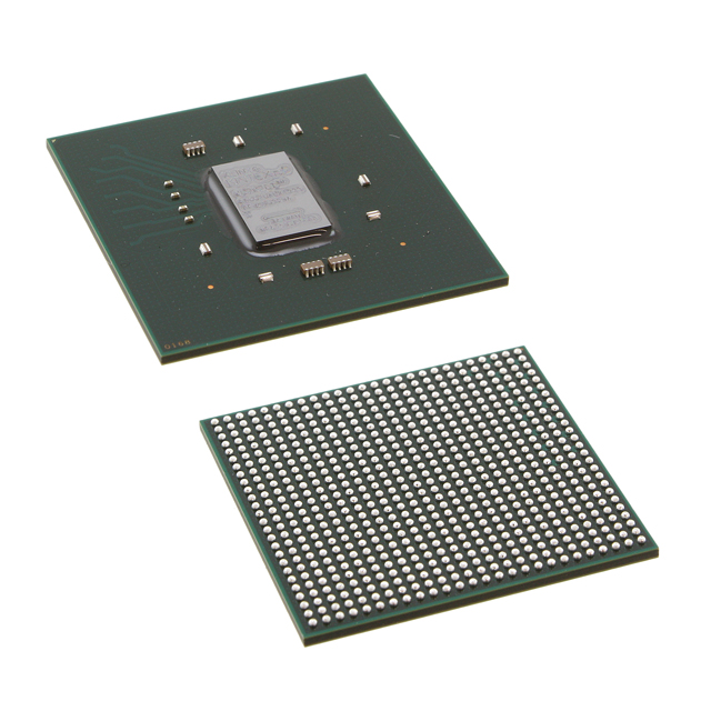
The XC7K325T-2FFG900C is a Kintex®-7 Field Programmable Gate Array (FPGA) from AMD offering high logic capacity and on-chip memory in a 900-ball FCBGA package. Key device resources include 326,080 logic elements, approximately 16.4 Mbits of embedded memory, and 500 user I/O pins, all designed for surface-mount assembly.
Electrical and environmental parameters include a core supply voltage range of 0.970 V to 1.03 V and an operating temperature range of 0 °C to 85 °C. The device is delivered in a 900-FCBGA (31 × 31) package and is RoHS compliant.
Key Features
- Core Logic 326,080 logic elements provide substantial programmable logic capacity for complex designs and implementation flexibility.
- Embedded Memory Approximately 16.4 Mbits of on-chip RAM for data buffering, state storage, and memory-intensive logic functions.
- High I/O Count 500 I/O pins to support dense interconnect and multiple high-pin-count peripherals or board-level interfaces.
- Package & Mounting 900-ball FCBGA package (900-FCBGA, 31×31) for compact board footprint; designed for surface-mount assembly.
- Power Specified core voltage supply range from 0.970 V to 1.03 V to match system power-rail planning.
- Operating Range & Grade Commercial grade device with an operating temperature range of 0 °C to 85 °C.
- Compliance RoHS compliant for lead-free manufacturing processes.
Typical Applications
- High-density logic implementations — Use the large pool of 326,080 logic elements to implement complex FPGA-based state machines, datapaths, and custom accelerators.
- Memory-intensive functions — Approximately 16.4 Mbits of embedded RAM enables on-chip buffering, FIFO structures, and local data storage for streaming or packet-processing designs.
- Multi-interface systems — 500 user I/O pins support multiple parallel and serial interfaces, enabling integration with a variety of peripherals and daughter cards.
Unique Advantages
- High logic capacity: 326,080 logic elements enable consolidation of multiple functions into a single FPGA, reducing component count and board complexity.
- Substantial on-chip memory: Approximately 16.4 Mbits of embedded RAM supports data buffering and local algorithm state without immediate external memory dependence.
- Extensive I/O: 500 I/O pins allow flexible partitioning of signals and support for multiple interfaces or parallel buses on the same device.
- Compact, surface-mount package: 900-FCBGA (31×31) package provides a high-pin-count solution in a compact footprint for dense board designs.
- Commercial operating range: Specified 0 °C to 85 °C operating temperature and RoHS compliance simplify integration into commercial electronic products.
- Tight core voltage specification: Core supply range of 0.970 V to 1.03 V aids in precise power-supply design and thermal planning.
Why Choose XC7K325T-2FFG900C?
The XC7K325T-2FFG900C positions itself as a high-capacity Kintex®-7 FPGA option for commercial designs that require substantial programmable logic, on-chip memory, and large I/O counts in a compact FCBGA package. Its combined resource profile—326,080 logic elements, ~16.4 Mbits of RAM, and 500 I/Os—supports integration of sizable digital functions onto a single device.
This device suits engineers looking for a commercially graded FPGA with clear electrical and thermal specifications, RoHS compliance, and a high-density package format. It delivers design scalability and the on-chip resources needed for complex logic, buffering, and interfacing requirements.
Request a quote or submit a quote to discuss availability, lead times, and pricing for the XC7K325T-2FFG900C. Our team can assist with ordering and supply details.

























Date Founded: 1969
Headquarters: Santa Clara, California, USA
Employees: 25,000+
Revenue: $22.68 Billion
Certifications and Memberships: ISO9001:2015, RoHS, REACH











