
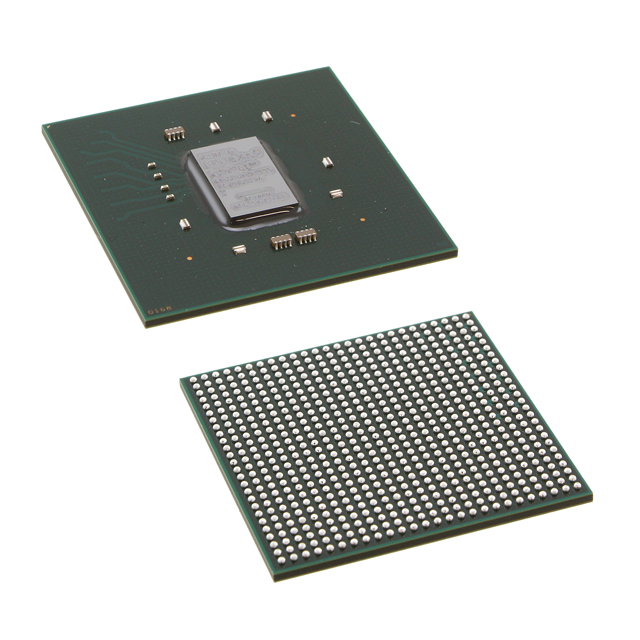
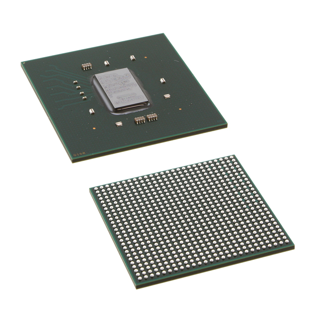
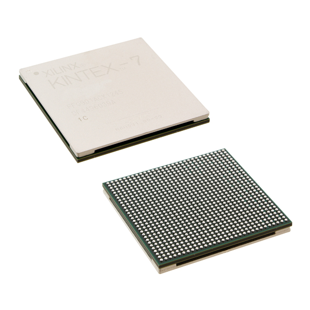
XC7K410T-2FFG676C
| Part Description |
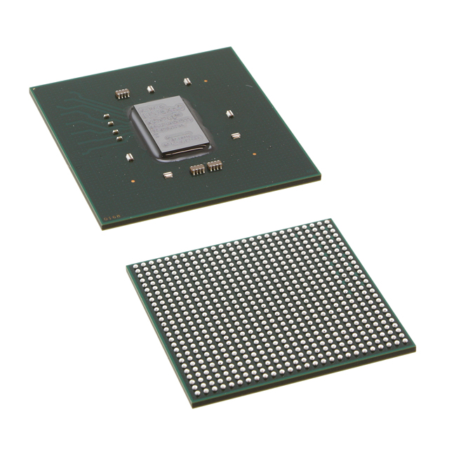
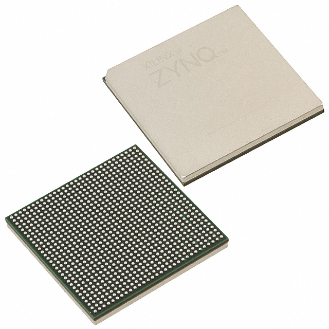
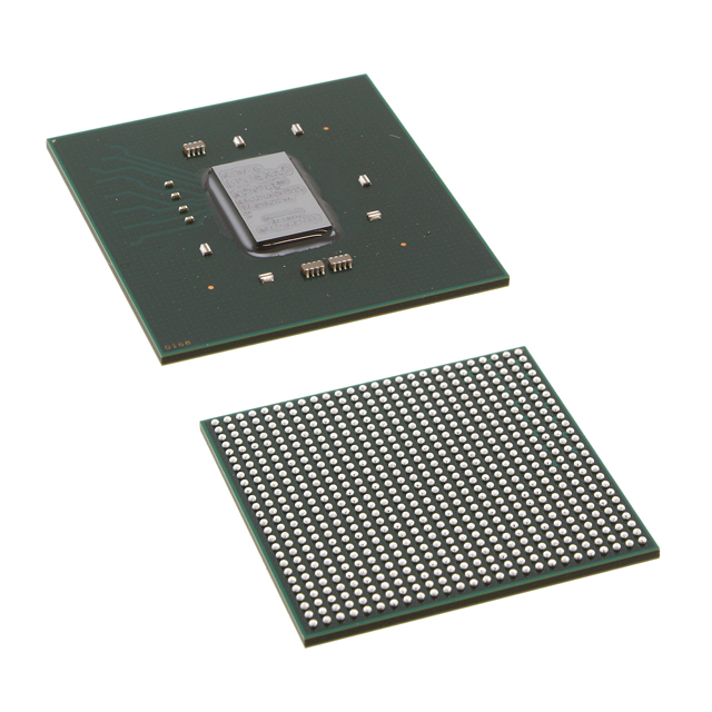
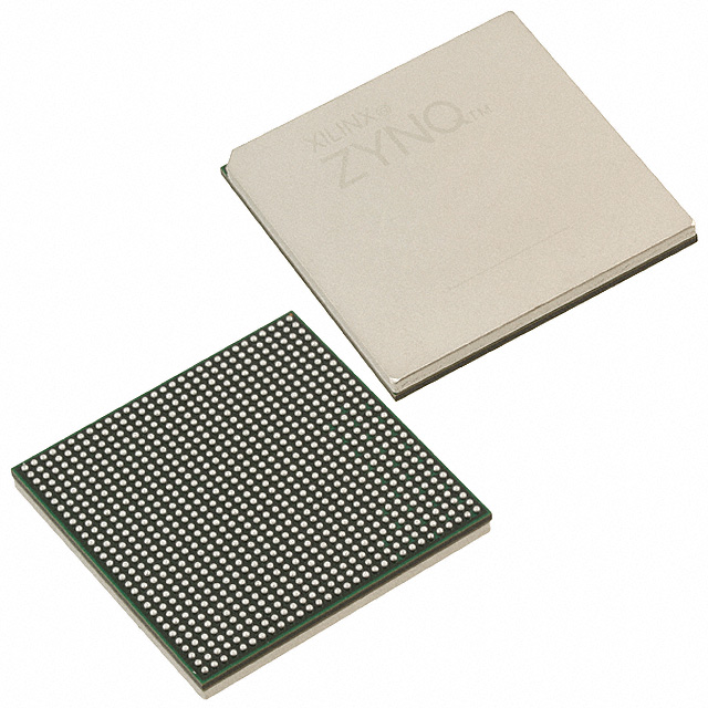
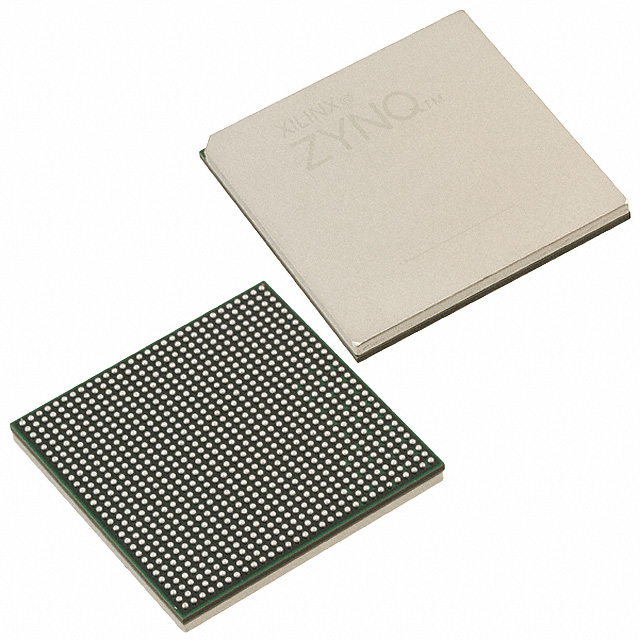
Kintex®-7 Field Programmable Gate Array (FPGA) IC 400 29306880 406720 676-BBGA, FCBGA |
|---|---|
| Quantity | 698 Available (as of October 8, 2026) |
| Product Category | Field Programmable Gate Array (FPGA) |
|---|---|
| Manufacturer | AMD |
| Manufacturing Status | Active |
| Manufacturer Standard Lead Time | 16 Weeks |
| Datasheet |
Specifications & Environmental
| Device Package | 676-FCBGA (27x27) | Grade | Commercial | Operating Temperature | 0°C – 85°C | ||
|---|---|---|---|---|---|---|---|
| Package / Case | 676-BBGA, FCBGA | Number of I/O | 400 | Voltage | 970 mV - 1.03 V | ||
| Mounting Method | Surface Mount | RoHS Compliance | ROHS3 Compliant | REACH Compliance | REACH Unaffected | ||
| Moisture Sensitivity Level | 4 (72 Hours) | Number of LABs/CLBs | 31775 | Number of Logic Elements/Cells | 406720 | ||
| Number of Gates | N/A | ECCN | 3A991D | HTS Code | 8542.39.0001 | ||
| Qualification | N/A | Total RAM Bits | 29306880 |
Overview of XC7K410T-2FFG676C – Kintex®-7 FPGA (400 I/Os, 676‑FCBGA)
The XC7K410T-2FFG676C is a Kintex®-7 field programmable gate array (FPGA) offered in a 676‑ball FCBGA package. It delivers large on‑chip logic and memory resources along with a broad I/O count for complex, system‑level designs.
This device targets designs that require substantial programmable logic and embedded memory while operating within commercial temperature ranges. Its combination of CLBs, logic elements, embedded RAM and a 27×27 mm FCBGA package supports dense, board‑level integration.
Key Features
- Kintex®-7 FPGA core Implement custom digital logic with 31,775 CLBs and 406,720 logic elements for complex designs.
- Embedded memory Approximately 29.3 Mbits of on‑chip RAM to support large buffers, state machines and data‑path storage.
- High I/O count 400 general‑purpose I/Os to enable extensive board connectivity and parallel interfaces.
- Power supply range Core supply specified from 970 mV to 1.03 V for defined operating conditions.
- Commercial temperature and grade Rated for 0 °C to 85 °C ambient operation and specified as Commercial grade.
- Package and mounting 676‑BBGA (FCBGA) package with supplier device package 676‑FCBGA (27×27 mm); surface mount assembly.
- Environmental compliance RoHS compliant for restriction of hazardous substances in manufacturing.
Typical Applications
- Custom digital logic implementations — Provides substantial CLB and logic element counts for tailored state machines, control logic and glue‑logic tasks.
- Memory‑intensive designs — Approximately 29.3 Mbits of embedded RAM supports buffering, packet storage and local data caching.
- I/O‑rich system integration — 400 I/Os enable integration with multiple peripherals, sensors and board‑level interfaces.
- Board‑level prototyping and integration — Surface‑mount 676‑FCBGA package and defined supply range simplify placement in compact, production‑oriented PCB designs.
Unique Advantages
- Large programmable fabric: 31,775 CLBs and 406,720 logic elements provide the headroom to implement complex logic and parallel datapaths on a single device.
- Significant embedded memory: Approximately 29.3 Mbits of on‑chip RAM reduces external memory dependence for many buffering and data‑processing tasks.
- Extensive I/O capability: 400 I/Os give designers flexibility to connect multiple peripherals, sensors and interfaces without sacrificing pin budget.
- Compact, production‑ready package: 676‑FCBGA (27×27 mm) surface‑mount package supports high‑density PCB layouts and automated assembly processes.
- Clear electrical and thermal bounds: Specified core voltage range (970 mV–1.03 V) and commercial temperature rating (0 °C–85 °C) help define system power and thermal design parameters.
- RoHS compliance: Meets environmental requirements for modern electronics manufacturing.
Why Choose XC7K410T-2FFG676C?
The XC7K410T-2FFG676C positions itself as a high‑capacity Kintex®‑7 FPGA option for designers who need significant logic and memory resources combined with a large number of I/Os in a compact FCBGA package. Its specified core voltage range and commercial temperature rating make it straightforward to integrate into board‑level designs where defined electrical and thermal parameters are required.
This part is well suited for teams building complex, memory‑heavy digital systems or consolidating multiple functions into a single programmable device. Selecting this FPGA provides scalability in logic and memory resources while maintaining clear manufacturing and environmental compliance characteristics.
Request a quote or submit a purchase inquiry for the XC7K410T-2FFG676C to obtain pricing and availability information tailored to your project needs.





















Date Founded: 1969
Headquarters: Santa Clara, California, USA
Employees: 25,000+
Revenue: $22.68 Billion
Certifications and Memberships: ISO9001:2015, RoHS, REACH











