
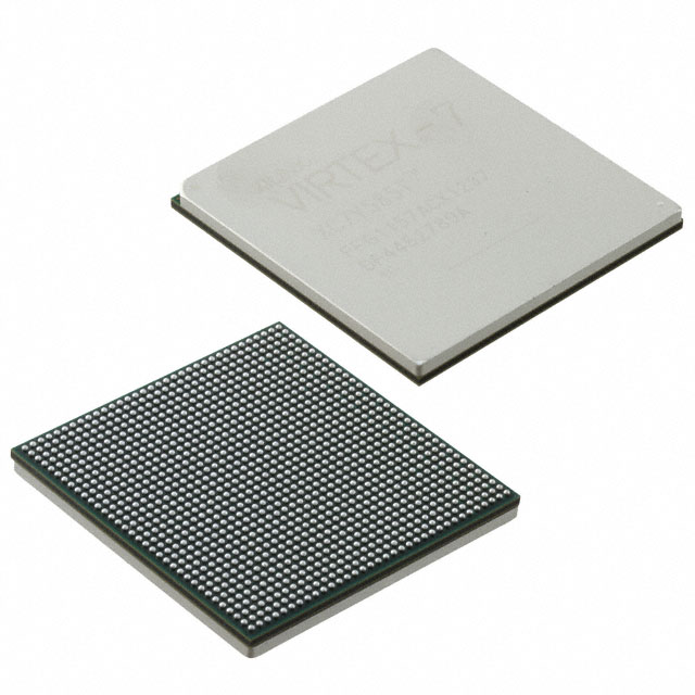
XC7VX485T-L2FFG1157E
| Part Description |
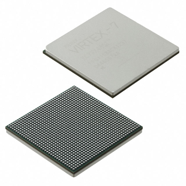
Virtex®-7 XT Field Programmable Gate Array (FPGA) IC 600 37969920 485760 1156-BBGA, FCBGA |
|---|---|
| Quantity | 569 Available (as of October 8, 2026) |
| Product Category | Field Programmable Gate Array (FPGA) |
|---|---|
| Manufacturer | AMD |
| Manufacturing Status | Active |
| Manufacturer Standard Lead Time | 16 Weeks |
| Datasheet |
Specifications & Environmental
| Device Package | 1157-FCBGA (35x35) | Grade | Extended | Operating Temperature | 0°C – 100°C | ||
|---|---|---|---|---|---|---|---|
| Package / Case | 1156-BBGA, FCBGA | Number of I/O | 600 | Voltage | 970 mV - 1.03 V | ||
| Mounting Method | Surface Mount | RoHS Compliance | ROHS3 Compliant | REACH Compliance | REACH Unaffected | ||
| Moisture Sensitivity Level | 4 (72 Hours) | Number of LABs/CLBs | 37950 | Number of Logic Elements/Cells | 485760 | ||
| Number of Gates | N/A | ECCN | 3A001A7A | HTS Code | 8542.39.0001 | ||
| Qualification | N/A | Total RAM Bits | 37969920 |
Overview of XC7VX485T-L2FFG1157E – Virtex®-7 XT FPGA, 1156‑BBGA (FCBGA)
The XC7VX485T-L2FFG1157E is a Virtex®-7 XT field programmable gate array (FPGA) IC from AMD, optimized for high-density programmable logic and extensive I/O integration. With hundreds of thousands of logic elements and tens of megabits of embedded memory, it addresses complex digital designs that require large on-chip resources and flexible system interfacing.
Suited for applications that demand significant logic capacity, substantial embedded RAM, and a high I/O count, this device provides a balanced platform for system architects focused on integration, scalability, and predictable operating parameters.
Key Features
- Logic Capacity Approximately 485,760 logic elements, enabling large, complex designs and deep logic integration on a single device.
- Embedded Memory Approximately 38 Mbits of on-chip RAM (37,969,920 total RAM bits) to support data buffering, packet processing, and algorithm state storage without external memory dependence.
- I/O Density 600 general-purpose I/O pins suitable for high-channel-count interfaces, parallel buses, and multi-lane data connections.
- Supply Voltage Core voltage specified from 970 mV to 1.03 V, enabling precise power budgeting for system-level integration.
- Thermal and Grade Extended grade device with an operating temperature range of 0 °C to 100 °C for deployment in commercial and extended-temperature environments.
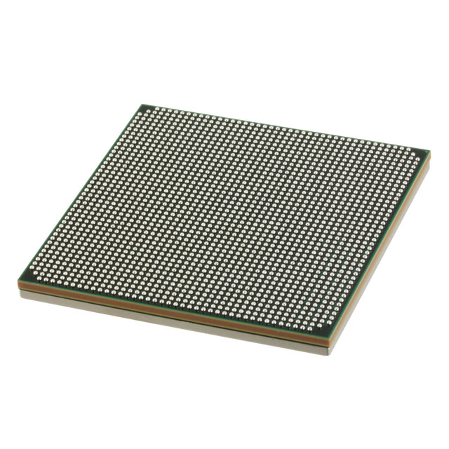
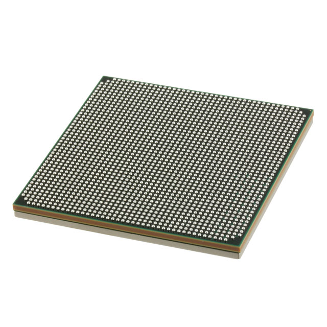
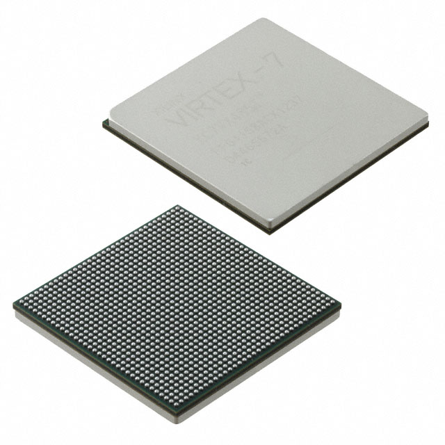
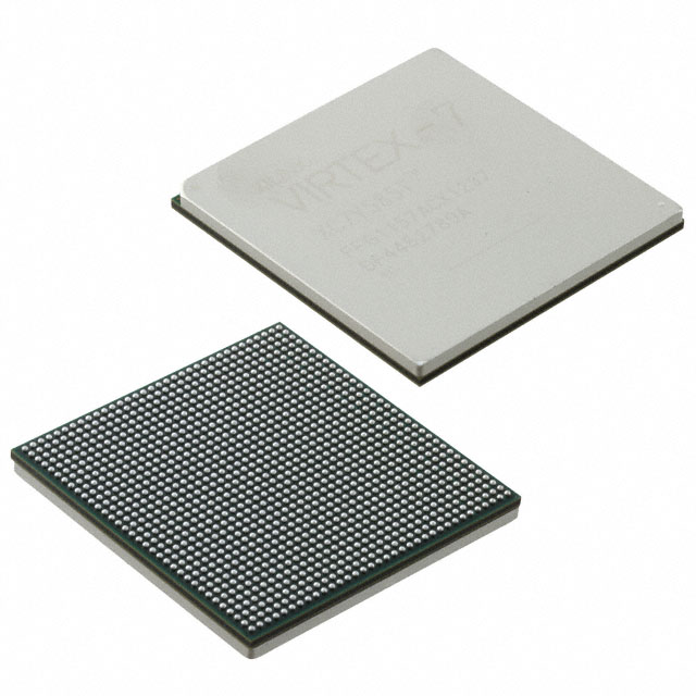
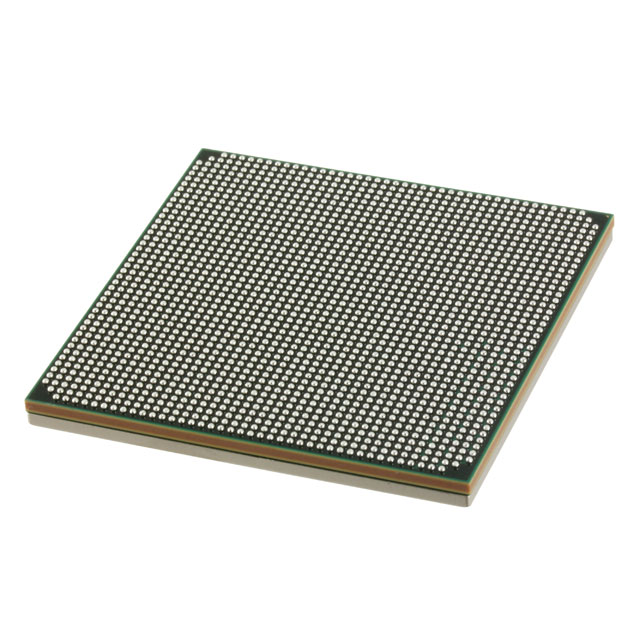
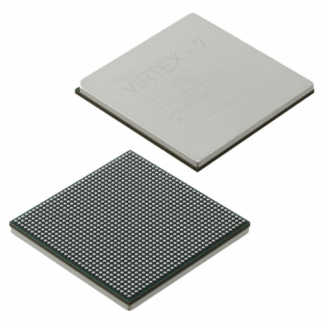
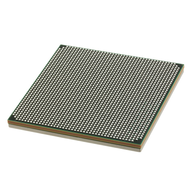
- Package and Mounting 1156‑BBGA, FCBGA package specified; supplier device package listed as 1157‑FCBGA (35×35). Surface-mount mounting type supports standard PCB assembly processes.
- High Logic Block Count Listed logic block count of 37,950 to complement the device's substantial logic-element budget for partitioned or hierarchical designs.
- RoHS Compliant Manufactured to meet RoHS environmental requirements.
Typical Applications
- Communications and Networking Large I/O count and abundant on-chip RAM enable packet processing, protocol bridging, and configurable datapath implementations.
- Video and Broadcast Processing High logic density and embedded memory support real-time video pipelines, frame buffering, and custom image-processing blocks.
- Test and Measurement Flexible logic resources and many I/O pins are well suited for custom instrumentation, data acquisition, and signal conditioning front ends.
- Compute Acceleration and Dataflow Substantial logic and memory resources support implementation of application-specific acceleration engines and parallel processing fabrics.
Unique Advantages
- High logic integration: Approximately 485,760 logic elements enable consolidation of multiple functions onto a single FPGA, reducing system BOM and interconnect complexity.
- Significant on-chip memory: Around 38 Mbits of embedded RAM reduces reliance on external memory, improving latency and simplifying board-level design.
- Extensive I/O availability: 600 I/O pins accommodate dense interfacing requirements for multi-channel systems and high-bandwidth I/O topologies.
- Controlled supply window: Core voltage specified from 0.97 V to 1.03 V allows predictable power design and rail planning at the system level.
- Surface-mount FCBGA packaging: 1156‑BBGA / 1157‑FCBGA options provide a compact, high-density package suitable for modern PCB layouts.
- Extended-grade operation: Rated for 0 °C to 100 °C, offering stable performance across commercial and extended-temperature use cases.
Why Choose XC7VX485T-L2FFG1157E?
The XC7VX485T-L2FFG1157E combines large-scale programmable logic, substantial embedded memory, and a high I/O count in a surface-mount FCBGA package, making it a strong candidate for designs that require on-chip integration of multiple functions and dense external interfacing. Its specified voltage range and extended operating temperature provide clear parameters for system power and thermal design.
This device is well suited to engineers and system designers building complex digital platforms—where consolidation of functionality, deterministic on-chip resources, and a clear packaging footprint matter for board-level integration and long-term design scalability.
Request a quote or submit a product inquiry to obtain pricing, availability, and ordering details for the XC7VX485T-L2FFG1157E.





















Date Founded: 1969
Headquarters: Santa Clara, California, USA
Employees: 25,000+
Revenue: $22.68 Billion
Certifications and Memberships: ISO9001:2015, RoHS, REACH











