
XCKU040-1FBVA676C
| Part Description |
Kintex® UltraScale™ Field Programmable Gate Array (FPGA) IC 312 21606000 530250 676-BBGA, FCBGA |
|---|---|
| Quantity | 63 Available (as of June 10, 2026) |

| Product Category | Field Programmable Gate Array (FPGA) |
|---|---|
| Manufacturer | AMD |
| Manufacturing Status | Active |
| Manufacturer Standard Lead Time | 16 Weeks |
| Datasheet |
Specifications & Environmental
| Device Package | 676-FCBGA (27x27) | Grade | Commercial | Operating Temperature | 0°C – 85°C | ||
|---|---|---|---|---|---|---|---|
| Package / Case | 676-BBGA, FCBGA | Number of I/O | 312 | Voltage | 922 mV - 979 mV | ||
| Mounting Method | Surface Mount | RoHS Compliance | ROHS3 Compliant | REACH Compliance | REACH Unaffected | ||
| Moisture Sensitivity Level | 4 (72 Hours) | Number of LABs/CLBs | 30300 | Number of Logic Elements/Cells | 530250 | ||
| Number of Gates | N/A | ECCN | 3A991D | HTS Code | 8542.39.0001 | ||
| Qualification | N/A | Total RAM Bits | 21606000 |
Overview of XCKU040-1FBVA676C – Kintex® UltraScale™ FPGA, 676-FCBGA, 312 I/O
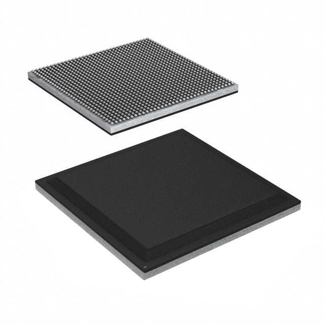
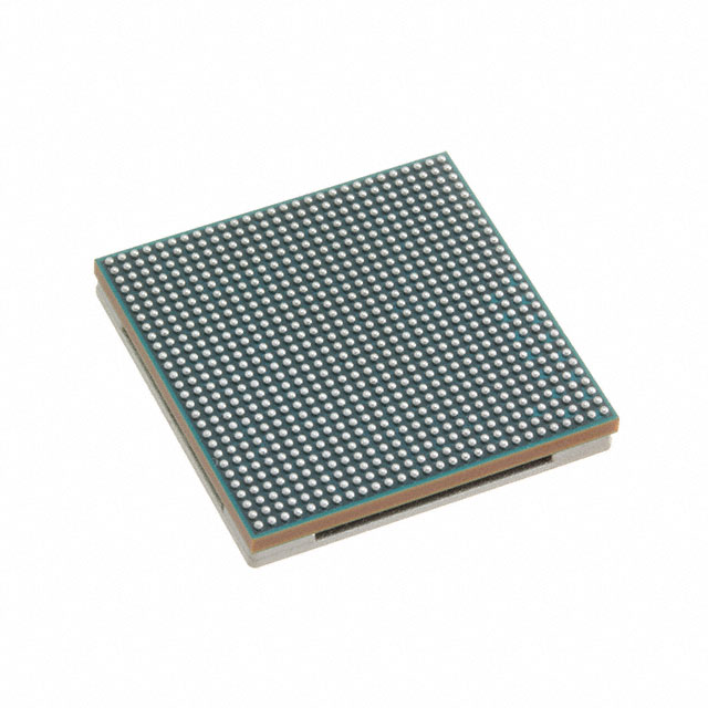
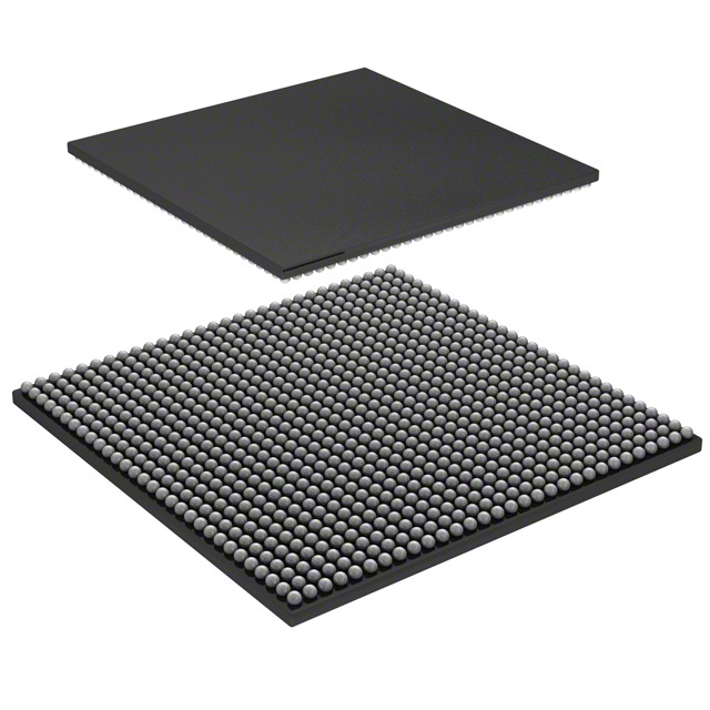
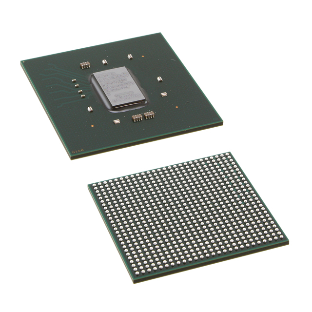
The XCKU040-1FBVA676C is a Kintex® UltraScale™ field programmable gate array (FPGA) from AMD supplied in a 676-ball FCBGA package. It combines high logic capacity and sizeable on-chip RAM with a 312-pin I/O footprint and is supplied in a surface-mount FCBGA (27 × 27 mm) package.
This commercial-grade device is specified for single-supply operation in the 922 mV to 979 mV range and an ambient operating temperature of 0 °C to 85 °C, delivering reconfigurable logic resources and embedded memory for a range of system-level designs.
Key Features
- Logic Capacity Approximately 530,250 logic elements to implement complex, reconfigurable digital logic and custom accelerators.
- Configurable Logic Blocks Approximately 30,300 configurable logic blocks (CLBs) for flexible partitioning of logic and routing resources.
- Embedded Memory Approximately 21.6 Mbits of on-chip RAM to support buffering, large lookup tables, and memory-intensive functions.
- I/O Resources 312 user I/O pins, enabling broad interfacing options for high-pin-count systems and multi-channel designs.
- Power Specified core supply range from 922 mV to 979 mV to match platform power domains and regulator targets.
- Package & Mounting 676-ball FCBGA (27 × 27 mm) package, surface mount, suitable for compact board layouts with high pin density.
- Grade & Temperature Commercial grade with an operating temperature range of 0 °C to 85 °C for standard embedded and computing applications.
- Environmental Compliance RoHS compliant.
Typical Applications
- Compute Acceleration Implement custom data-paths and hardware accelerators where high logic density and embedded RAM improve throughput.
- Networking & Communications Use the device’s plentiful I/O and reconfigurable logic to implement protocol processing, packet inspection, and interface bridging.
- Signal Processing Leverage the large embedded memory and logic resources for real-time DSP, filtering, and multi-channel data handling.
- Prototyping & System Integration Rapidly iterate system-level designs and integrate IP blocks on a single, high-capacity FPGA platform.
Unique Advantages
- High Logic Density: With roughly 530,250 logic elements, the device supports complex system integration on a single FPGA.
- Substantial On-Chip Memory: Approximately 21.6 Mbits of embedded RAM reduces the need for external memory in many buffering and streaming use cases.
- Generous I/O Count: 312 user I/Os provide flexibility for multi-protocol interfaces, parallel data lanes, and high-pin-count peripherals.
- Compact, High-Pin Package: The 676-FCBGA (27 × 27 mm) footprint balances board space efficiency with dense pin access for system routing.
- Commercial Temperature Rating: Rated for 0 °C to 85 °C operation to meet standard embedded and computing environment requirements.
- Regulatory-Friendly: RoHS compliance supports environmental and manufacturing requirements.
Why Choose XCKU040-1FBVA676C?
The XCKU040-1FBVA676C provides a balanced combination of high logic element count, substantial embedded memory, and a high I/O complement in a compact FCBGA package. This balance makes it well suited to system designs that require significant on-chip processing, buffering, and interface density without expanding board area.
Manufactured by AMD and offered as a commercial-grade FPGA, this part is appropriate for engineering teams and procurement seeking a reconfigurable platform for compute acceleration, signal processing, communications, and advanced prototyping where on-chip capacity and I/O flexibility are primary selection criteria.
Request a quote or submit a parts inquiry for the XCKU040-1FBVA676C to check availability and pricing for your design requirements.


Date Founded: 1969
Headquarters: Santa Clara, California, USA
Employees: 25,000+
Revenue: $22.68 Billion
Certifications and Memberships: ISO9001:2015, RoHS, REACH


