
XCKU085-2FLVA1517I
| Part Description |
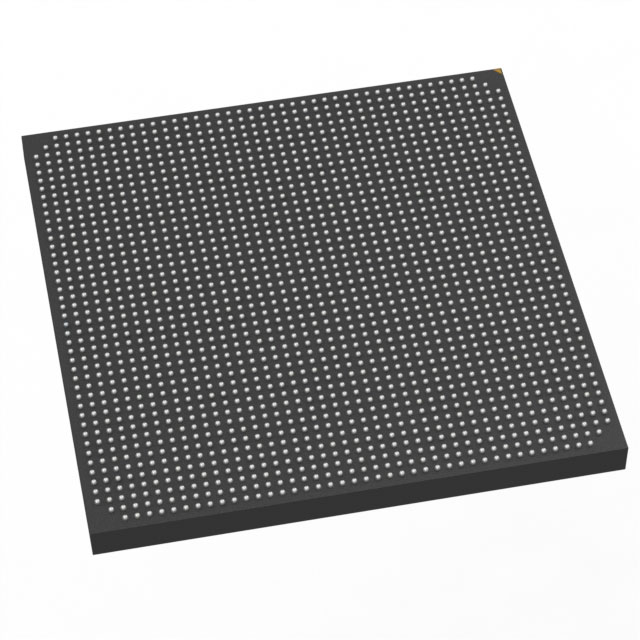
Kintex® UltraScale™ Field Programmable Gate Array (FPGA) IC 624 58265600 1088325 1517-BBGA, FCBGA |
|---|---|
| Quantity | 525 Available (as of June 10, 2026) |

| Product Category | Field Programmable Gate Array (FPGA) |
|---|---|
| Manufacturer | AMD |
| Manufacturing Status | Active |
| Manufacturer Standard Lead Time | 20 Weeks |
| Datasheet |
Specifications & Environmental
| Device Package | 1517-FCBGA (40x40) | Grade | Industrial | Operating Temperature | -40°C – 100°C | ||
|---|---|---|---|---|---|---|---|
| Package / Case | 1517-BBGA, FCBGA | Number of I/O | 624 | Voltage | 922 mV - 979 mV | ||
| Mounting Method | Surface Mount | RoHS Compliance | ROHS3 Compliant | REACH Compliance | REACH Unaffected | ||
| Moisture Sensitivity Level | 4 (72 Hours) | Number of LABs/CLBs | 62190 | Number of Logic Elements/Cells | 1088325 | ||
| Number of Gates | N/A | ECCN | 3A001A7B | HTS Code | 8542.39.0001 | ||
| Qualification | N/A | Total RAM Bits | 58265600 |
Overview of XCKU085-2FLVA1517I – Kintex® UltraScale™ FPGA, 1517-FCBGA (40×40)
The XCKU085-2FLVA1517I is a Kintex® UltraScale™ field programmable gate array (FPGA) IC from AMD offered in a 1517-ball FCBGA package. It provides very high logic density and substantial on-chip RAM to support complex, resource-intensive FPGA designs.
Key on-chip resources include approximately 1,088,325 logic elements and about 58.3 Mbits of embedded memory, together with 624 user I/O pins. The device is specified for industrial-grade use with a supply range of 922 mV to 979 mV and an operating temperature range of –40 °C to 100 °C.
Key Features
- Core density Approximately 1,088,325 logic elements, providing high implementation capacity for large, parallel logic designs.
- Embedded memory Approximately 58.3 Mbits of on-chip RAM for buffering, lookup tables, and storage close to logic.
- Programmable I/O 624 I/O pins to support broad external interface requirements and board-level connectivity.
- Power supply range Specified supply voltage from 922 mV to 979 mV for core power planning and system integration.
- Industrial temperature and grade Industrial-grade device rated for –40 °C to 100 °C operation.
- Package & mounting 1517-ball FCBGA package (supplier package: 1517-FCBGA (40×40)), surface-mount configuration for dense PCB integration.
Unique Advantages
- High logic capacity: The large logic element count supports dense designs and complex finite-state machines or datapaths.
- Substantial on-chip memory: Approximately 58.3 Mbits of embedded RAM reduces external memory dependence and shortens data paths.
- Extensive I/O availability: 624 user I/Os enable flexible interfacing to peripherals and multiple board-level signals.
- Industrial robustness: Rated for operation from –40 °C to 100 °C, suitable for demanding thermal environments.
- Compact surface-mount package: 1517-FCBGA (40×40) packaging supports high-density board layouts while maintaining a predictable footprint.
Why Choose XCKU085-2FLVA1517I?
The XCKU085-2FLVA1517I combines a high logic element count and significant embedded memory with a large complement of I/Os to address designs that require substantial on-chip resources in an industrial-grade FPGA package. Its specified voltage and temperature ranges allow straightforward integration into systems with defined power domains and environmental requirements.
Manufactured by AMD and offered in a 1517-FCBGA surface-mount package, this device is suited to projects that need scalable logic capacity and ample on-chip RAM while maintaining rugged operation across a wide temperature range.
Request a quote or submit an inquiry to receive pricing and availability information for the XCKU085-2FLVA1517I.


Date Founded: 1969
Headquarters: Santa Clara, California, USA
Employees: 25,000+
Revenue: $22.68 Billion
Certifications and Memberships: ISO9001:2015, RoHS, REACH


