
XCVU190-3FLGA2577E
| Part Description |
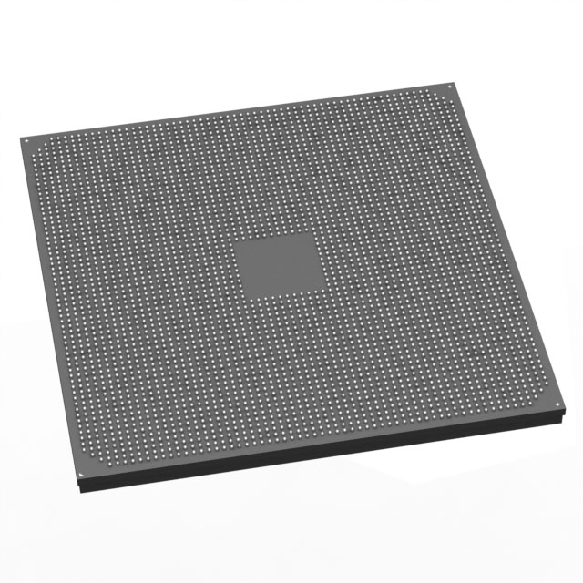
Virtex® UltraScale™ Field Programmable Gate Array (FPGA) IC 448 150937600 2349900 2577-BBGA, FCBGA |
|---|---|
| Quantity | 546 Available (as of June 9, 2026) |

| Product Category | Field Programmable Gate Array (FPGA) |
|---|---|
| Manufacturer | AMD |
| Manufacturing Status | Active |
| Manufacturer Standard Lead Time | 20 Weeks |
| Datasheet |
Specifications & Environmental
| Device Package | 2577-FCBGA (52.5x52.5) | Grade | Extended | Operating Temperature | 0°C – 100°C | ||
|---|---|---|---|---|---|---|---|
| Package / Case | 2577-BBGA, FCBGA | Number of I/O | 448 | Voltage | 970 mV - 1.03 V | ||
| Mounting Method | Surface Mount | RoHS Compliance | ROHS3 Compliant | REACH Compliance | REACH Unknown | ||
| Moisture Sensitivity Level | 4 (72 Hours) | Number of LABs/CLBs | 134280 | Number of Logic Elements/Cells | 2349900 | ||
| Number of Gates | N/A | ECCN | 3A001A7B | HTS Code | 8542.39.0001 | ||
| Qualification | N/A | Total RAM Bits | 150937600 |
Overview of XCVU190-3FLGA2577E – Virtex® UltraScale™ FPGA, 2577-FCBGA (52.5×52.5)
The XCVU190-3FLGA2577E is a Virtex® UltraScale™ Field Programmable Gate Array (FPGA) IC delivering very high programmable logic capacity and substantial on-chip memory in a 2577-ball FCBGA package. It provides a large number of logic elements and embedded RAM suited to designs that require dense programmable fabric and significant local memory resources.
With a supply range of 970 mV to 1.03 V, 448 I/O pins, and an operating temperature range of 0 °C to 100 °C, this extended-grade device addresses applications that need high integration and deterministic on-board resources in a surface-mount FCBGA form factor.
Key Features
- Programmable Logic Capacity Contains 2,349,900 logic elements to support large, complex FPGA designs and high-density logic implementation.
- Embedded Memory Approximately 150.9 Mbits of on-chip RAM to accommodate large buffering, lookup tables, and memory-intensive logic functions.
- I/O Density 448 configurable I/O pins for broad external connectivity and flexible interfacing to system peripherals and high-speed buses.
- Power Domain Core voltage range of 970 mV to 1.03 V, enabling operation within the specified power envelope for the device.
- Package and Mounting 2577-BBGA / 2577-FCBGA package (52.5×52.5 mm) in a surface-mount format for high-density board integration.
- Temperature and Grade Extended-grade device rated for operation from 0 °C to 100 °C, suitable for applications requiring this temperature specification.
- Compliance RoHS compliant, meeting environmental substance requirements for lead-free assembly processes.
Typical Applications
- High-density FPGA designs — Large-scale programmable systems that require millions of logic elements and extensive on-chip RAM to implement complex custom logic.
- Memory-intensive processing — Designs that leverage approximately 150.9 Mbits of embedded RAM for buffering, lookup tables, or local data storage.
- Interface consolidation — Systems that need a large number of I/O (448 pins) to aggregate, translate, or bridge multiple external interfaces on a single device.
Unique Advantages
- High logic density: 2,349,900 logic elements enable consolidation of large functions and reduce the need for multiple devices.
- Substantial on-chip RAM: Approximately 150.9 Mbits of embedded memory supports local data handling and reduces external memory dependency.
- Robust I/O count: 448 I/O pins provide flexibility for extensive external connectivity and system integration options.
- Compact package: 2577-FCBGA (52.5×52.5 mm) surface-mount package allows high-density board designs while accommodating the device’s resources.
- Extended temperature rating: 0 °C to 100 °C operational range addresses designs requiring this specific temperature envelope.
- RoHS compliant: Meets environmental regulations for lead-free manufacturing and assembly.
Why Choose XCVU190-3FLGA2577E?
The XCVU190-3FLGA2577E positions itself as a high-capacity Virtex® UltraScale™ FPGA option that balances extensive logic resources, significant embedded memory, and a large I/O complement in a single FCBGA package. Its specifications support designs that demand dense programmable fabric and on-chip RAM while maintaining a defined power and thermal operating window.
This device is suited for engineers and teams developing complex programmable systems who need a scalable, high-integration FPGA platform. The combination of logic capacity, memory, I/O density, and RoHS compliance provides a clear foundation for robust designs that plan for long-term deployment and integration into dense PCBs.
Request a quote or submit a request to receive pricing and availability information for the XCVU190-3FLGA2577E.


Date Founded: 1969
Headquarters: Santa Clara, California, USA
Employees: 25,000+
Revenue: $22.68 Billion
Certifications and Memberships: ISO9001:2015, RoHS, REACH


